AL5068S Designer’s Guide ISDN Socket Modem AL5068S, AL5068S-3V Series Designer’s Guide RELEASED 13. SEPTEMBER 2006 No.
AL5068S Designer’s Guide Information provided by Altec Electronic AG is believed to be accurate and reliable. However, no responsibility is assumed by Altec Electronic for its use, nor any infringement of patents or other rights of third parties which may result from its use. No license is granted by implication or otherwise under any patent rights of Altec Electronic other than for circuitry embodied in Altec products. Altec Electronic reserves the right to change circuitry at any time without notice.
AL5068S Designer’s Guide TABLE OF CONTENTS 1. INTRODUCTION ................................................................................................. 5 1.1 1.2 1.3 1.4 2. Overview ...................................................................................................... 5 Product description....................................................................................... 5 Features ..................................................................................................
AL5068S Designer’s Guide List of Figures FIGURE 1-1. TYPICAL SERIAL BLOCK DIAGRAMS ................................................ 8 FIGURE 3.1 – SERIAL TTL PINOUT ....................................................................... 11 FIGURE 4-1. AL5068S SOCKET MODEM PHYSICAL DIMENSIONS ................... 22 List of Tables TABLE 3.1. SERIAL TTL SIGNALS ................................................................................. 11 TABLE 3.2 / SIGNAL DESCRIPTIONS ................................
AL5068S Designer’s Guide 1. INTRODUCTION 1.1 Overview This Designer’s Guide describes the hardware for the following ISDN socket modems of Altec Electronic AG: AL5068S AL5068S-3V AL5068SI-3V ISDN Socket Modem (5V Version) ISDN Socket Modem (3V Version) ISDN Socket Modem (3V Version and IOM-2 bus) The description apply to all these isdn-modems with any differences between product families noted. Refer to Modem Firmware Release notes for commands applicable to modem firmware.
AL5068S Designer’s Guide 1.3 Features • • • • • • • • • • • • • • • • • • • • • • • • 1.4 D-Channel Protocols: - DSS1 - X.31 (D-Channel) B-Channel Protocols: - HDLC transparent - PPP async-sync (RFC1662) - X.75, - V.120 - V.110 - X.31, X.25 ISDN S0 (I.430) Interface. Several Dial Procedures: - AT commands - Auto Connect X.3 PAD intergrated. Command Interpreters with standard AT Commands Trace Log Buffers. Caller ID access control.
AL5068S Designer’s Guide 2. TECHNICAL OVERVIEW 2.1 Dialing procedures The following dial procedures are supported: • AT commands • Auto-connect (Hotline call) • X.3 PAD 2.2 AT Commands Via AT-Commands you may control the ISDN connections and change the configuration of the AL5068S. ISDN specific configuration commands are supported. 2.2.
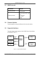
AL5068S Designer’s Guide 2.3 2.4 ISDN Protocols: ISDN Channel Protocols D-channel protocols: DSS1 X.31 D-channel B-channel protocols: HDLC (transparent) PPP sync-async (RFC 1662) X.75 Bit-transparent X.31 / X.25 V.110 V.120 Firmware Updates Firmware updates can always be affected via the local serial interface. 2.5 Supported Interfaces The major hardware signal interfaces of the AL5068S Series Socket Modem are illustrated in Figure 1-1.
AL5068S Designer’s Guide Serial / Indicator Interface: DTE serial interface and indicator outputs are supported. Serial Interface: 8-line TTL logic serial interface to the DTE is supported. LED Interface: Four direct connect LED indicator outputs are supported The terminal (DTE) baudrate is determined automatically by the MCU firmware. It provides autobaud from 9600bps to 115200bps. The terminal (DTE) character format is fixed to 8 bits, no parity and 1 stop bit.
AL5068S Designer’s Guide 3. HARDWARE INTERFACE 3.1 Interface Signals The ISDN Socket Modem pin assignments with DTE serial TTL interface are shown in Figure 3-1 and are listed in Table 3-1. 3.2 Signal Descriptions The Socket Modem interface signals are described in Table 3.2, 3.3 and 3.4. The digital electrical characteristics are listed in Table 3.5 The absolut maximum ratings are listed in Table 3-6. No.
AL5068S Designer’s Guide Figure 3.
AL5068S Designer’s Guide Table 3.2 / Signal Descriptions Label I/O Type Signal Name Description VCC PWR +5 VDC / 3.3 VDC GND GND Ground. Connect to Digital Ground on the interface circuit. ~RESET IC Modem Reset. The Active Low ~RESET input resets the Socket Modems logic and returns the AT command set to the original factory default values and to “stored values” in NVRAM. ~RESET is connected to a builtin reset circuit on the Socket Modem. This input is 5V tolerant.
AL5068S Designer’s Guide Table 3.4 / Serial Interface Signal Descriptions IA Request To Send (TTL Active Low). ~RTS is used to condition the local modem for data transmission and, during half-duplex operation, to control the direction of data transmission. On a full-duplex channel, RTS-OFF maintains the modem in a nontransmit mode. A non-transmit mode does not imply that the ISDN link have been terminated. RTS input ON causes the modem to transmit data on TXD when ~CTS becomes active.
AL5068S Designer’s Guide Table 3.5 / Digital Electrical Characteristics Parameter Symbol Input Voltage Min. Typ. Max. VI Type IA Type IC - 5.5 5.5 0 0 Input High Voltage - 3.3 3.3 VICH Type IA Type IC Vdc 2.0 2.0 Input Low Voltage - - VIL Type IA Type IC Vdc - Output High Voltage - 0.8 0.8 VOH Type OA Type OG Vdc 2.8 2.4 Output Low Voltage - ILOAD = -4.0 mA ILOAD = -1.
AL5068S Designer’s Guide Table 3.6 / Absolute Maximum Ratings Parameter Supply Voltage Symbol Max. -0.5 -0.5 - Test Condition +7.0 +3.6 Vdc VIN - +6.0 VDD 5V Version 3V Version Units Vdc -0.5 Nominal Supply Voltage Typ. VDD 5V Version 3V Version Input Voltage Min. Vdc 4.75 3.10 5.0 3.3 5.25 3.50 Static Discharge Voltage @ 25°C Operating Temperature Range VESD - TA °C 0 Storage Temperature Range - °C - +80 mA ID 19 Power 70 TSTG -40 Supply Current V +/- 2500 26 W W 0.
AL5068S Designer’s Guide 3.3 S0 INTERFACE The ISDN Socket Modem has all the necessary circuitry for the S0 Interface on-board, and is designed to meet the I.430 requirements of the European ISDN Network (S0 Bus). The TX+/- and RX+/- signals must be provided from the RJ45 Telco jack to pins 1 to 4 of the Socket Modem. The TX+/- and RX+/- signal traces are to be no closer than 2.5mm (0.1”) from any other traces on the main board.
AL5068S Designer’s Guide 3.4 External Reset Interface The AL5068S Socket Modem provides an external RESET input pin. This signal is used to force a reset procedure by providing low level during at least 100uS. This signal has to be considered as an emergency reset only. A reset procedure is already driven by an internal hardware during the powerup sequence. If no external reset is necessary this input can be left open. If used (emergency reset), it has to be driven by an open collector or an open drain.
AL5068S Designer’s Guide 3.5 IOM-2 Bus Interface The AL5068SI-3V ISDN Modem supports 2 independent analog channels by adding 2 external PCM Codecs. This Codecs are connected to the IOM-2 bus on pins 44…47 of the socket modem. It is possible to setup 2 simultaneous links for both incoming and outgoing calls. The serial port remains in command state in this mode. The 2 external Codecs are marked with Codec A and Codec B. Each Codec (A or B) can have his own MSN.
AL5068S Designer’s Guide 4. DESIGN CONSIDERATIONS Good engineering practices must be adhered to when designing a printed circuit board (PCB) containing the AL5068S Socket Modem module. Suppression of noise is essential to the proper operation and performance of the modem itself and for surrounding equipment.
AL5068S Designer’s Guide 4.1.2 Electromagnetic Interference (EMI) Considerations The following guidelines are offered to specifically help minimize EMI generation. Some of these guidelines are the same as, or similar to, the general guidelines but are mentioned again to reinforce their importance. In order to minimize the contribution of the Socket Modem-based design to EMI, the designer must understand the major sources of EMI and how to reduce them to acceptable levels. 1.
AL5068S Designer’s Guide 4.2 Manufacturing Considerations The Socket Modem has been designed to be mounted onto the host board in one of two ways. The first method consists of soldering two 32-pin strip sockets to the host board and inserting the Socket Modem into the sockets. A suggested part number for the 32-pin socket is Sam Tec SMM-132-01-F-S. The second way is to solder the Socket Modem directly to the host board. The most efficient way to do this is through a wave solder process.
AL5068S Designer’s Guide 5. PACKAGE DIMENSIONS Figure 4-1. AL5068S Socket Modem Physical Dimensions 26.5mm (1.04“) 64.5mm (2.54“) 7,6mm 1,6mm 2,0mm ∅0.5mm 24.0mm 6,5mm 62.0mm AL5068S Dimensions Width Height Length Weight Operating temperature Storage temperature Humidity No. AL5068S-E00-105 Europe 26,5 mm 14.1 mm 64,5 mm ~ 12 g 0...70 °C –10...85 °C 90% non-condensing Altec Electronic AG US ~1.05" ~0.55" ~2.55" ~ 0.42 oz 32...160 °F 14...
AL5068S Designer’s Guide 6. SOCKET MODEM APPROVALS The Socket Modem module is approved as a host-independent modem card. To maintain type approvals, permits and/or licenses valid, the guidelines described in this document must be followed. 6.1 Considerations for Telecom Approvals The Socket Modem has been assessed and has been found to comply with the relevant harmonized standards as defined by the European ETSI Directive (ETSI TC-TE). These standards are: TBR3 / CTR3 6.1.
AL5068S Designer’s Guide 6.3 Considerations for EMC 6.3.1 EMC Compliance (EU Countries) The Socket Modem has been assessed with respect to emission of and immunity to electromagnetic disturbances and has been found to comply with the relevant harmonized standards as defined by the European EMC Directive (89/336/EEC). These standards are: • Generic emission standards which refers to EN 55022:1998 +A1:2000, Class B • Generic immunity standards which refers to EN 55024:1999 6.3.
AL5068S Designer’s Guide 7. Appendix A 7.1 Schematic of external codecs C2 C1 0.01UF C3 0.1UF VCC3V 1 R3 20K R4 20K 2 3 4 PO1PO1+ 5 6 SOCKET MODEM B1/B2 19 20 21 22 7 R7 10K 8 C7 0.1UF 9 10 42 43 44 45 46 47 REF VAG RO- TI+ PI PO- U1 MC145481DW (Motorola) TITG MU/A PO+ VDD VSS FSR FST DR A DT BCLKT BCLKR MCLK PDI NA 20 19 R1 R2 10K 10K 18 R5 R6 16 10K 10K 15 C6 17 C4 1UF C5 PO1PO1+ 1 2 3 4 5 6 1UF ANALOG CH.