
Specifications


AL2094S Designers Guide
AL2094S-E00-102 xmodus swiss GmbH Seite 18 / 30
Table 3-3. Signal Descriptions (Cont'd)
Label Pin I/O I/O Type Signal Name/Description
RTS 34 I Ithpu
Request To Send (EIA CA/ITU-T CT105). RTS# input ON
(low) indicates that the DTE is ready to send data to the
modem. In the command state, the modem ignores RTS#.
In asynchronous operation, the modem ignores RTS# unless
RTS/CTS flow control is selected by the &Kn command. In
synchronous on-line operation, the modem can be
commanded by the &Rn command to ignore RTS# or to
respond to RTS# by turning on CTS# after the delay specified
by Register S26.
RXCLK 9 O Itpu/Ot2
Receive Data Clock. A synchronous Receive Data Clock
(RXCLK) is output in synchronous modes. The RXCLK
frequency is the data rate (±0.01%) with a duty cycle of
50±1%. Leave open if not used.
TXCLK 8 O Itpu/Ot2
Transmit Data Clock. A synchronous Transmit Data Clock
(TXCLK) is output in synchronous modes. The TXCLK
frequency is the data rate (±0.01%) with a duty cycle of
50±1%. Leave open if not used.
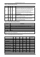
Table 3-4. AL2094S Modem I/O Type Definitions
I/O Type Description
It/Ot2 Digital input, +5V tolerant/ Digital output, 2 mA, ZINT = 120 Ω
Itpu/Ot2 Digital input, +5V tolerant, 75k Ω pull up/ Digital output, 2 mA, ZINT = 120 Ω
Ith/Ot8 Digital input, +5V tolerant, hysteresis/Digital output, 8 mA, ZINT = 50 Ω
It Digital input, +5V tolerant
Ithpu Digital input, +5V tolerant, hysteresis, 75k Ω pull up
IC/OC Open collector input/output, internal 10k pull-up
PWR VCC Power
GND Ground
NOTES:
I/O Type corresponds to the device Pad Type. The I/O column in signal interface tables refers to
signal I/O direction used in the application.
Table 3-5. AL2094S Modem DC Electrical Characteristics
Parameter Symbol Min Typ Max Units
Test
Conditions
Input Voltage Low VIL
+5V tolerant 0 - 0.8 V
+5V tolerant hysteresis 0 - 0.3 * VGG V
Input Voltage High VIH
+5V tolerant 2 - 5.25 V
+5V tolerant hysteresis 0.7 * VDD - 5.25 V
Input Hysteresis VH
+3V hysteresis 0.5 - V
+5V tolerant,hysteresis 0.3 - V
Output Voltage Low VOL
ZINT = 120 Ω 0 - 0.4 V IOL = 2 mA
ZINT = 50 Ω
0 - 0.4 V IOL = 8 mA
Output Voltage High VOH
ZINT = 120 Ω 2.4 - VDD V IOL = - 2 mA
ZINT = 50 Ω
2.4 - VDD V IOL = - 8 mA
Pull-Up Resistance Rpu 50 - 200 kΩ
Pull-Down Resistance Rpd 50 - 200 kΩ
Test Conditions unless otherwise stated: VDD = +3.3 ± 0.3 VDC; TA = 0°C to 70°C; external load = 50 pF.