
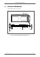
Specifications


AL2094S Designers Guide
AL2094S-E00-102 xmodus swiss GmbH Seite 24 / 30
4.1.2 Electromagnetic Interference (EMI) Considerations
The following guidelines are offered to specifically help minimize EMI generation. Some of
these guidelines are the same as, or similar to, the general guidelines but are mentioned
again to reinforce their importance.
In order to minimize the contribution of the Socket Modem-based design to EMI, the
designer must understand the major sources of EMI and how to reduce them to acceptable
levels.
1. Keep traces carrying high frequency signals as short as possible.
2. Provide a good ground plane or grid. In some cases, a multilayer board may be
required with full layers for ground and power distribution.
3. Decouple power from ground with decoupling capacitors as close to the Socket
Modem module power pins as possible.
4. Eliminate ground loops, which are unexpected current return paths to the power
source and ground.
5. Decouple the telephone line cables at the telephone line jacks. Typically, use a
combination of series inductors, common mode chokes, and shunt capacitors.
Methods to decouple telephone lines are similar to decoupling power lines, however,
telephone line decoupling may be more difficult and deserves additional attention. A
commonly used design aid is to place footprints for these components and populate
as necessary during performance/EMI testing and certification.
6. Decouple the power cord at the power cord interface with decoupling capacitors.
Methods to decouple power lines are similar to decoupling telephone lines.
7. Locate high frequency circuits in a separate area to minimize capacitive coupling to
other circuits.
8. Locate cables and connectors so as to avoid coupling from high frequency circuits.
10. If a mulilayer board design is used, make no cuts in the ground or power planes and
be sure the ground plane covers all traces.
11. Minimize the number of through-hole connections on traces carrying high frequency
signals.
12. Avoid right angle turns on high frequency traces. Forty-five degree corners are good,
however, radius turns are better
13. On 2-layer boards with no ground grid, provide a shadow ground trace on the opposite
side of the board to traces carrying high frequency signals. This will be effective as a
high frequency ground return if it is three times the width of the signal traces.
14. Distribute high frequency signals continuously on a single trace rather than several
traces radiating from one point.
4.2 Other Considerations
The pins of all Socket Modems are grouped according to function. The DAA interface, Host
interface, and LED interface pins are all conveniently arranged, easing the host board layout
design.
Altec Electronic has tested each of the SocketModems for compliance with their respective
country’s PTT requirements and has received PTT certificates that cover, without additional
expense to the user, all applications that use these Socket Modems in their respective
countries. The certificates apply only to designs that route TIP and RING (pins 20 and 21)
directly to the telco jack. Only specified EMI filtering components are allowed on these two
signals as shown in figure 3-3.