
Owner manual

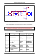


AL2094S Designers Guide
Doc. No. DG_2094E Altec Electronic AG Seite 23 / 30
4
4
.
.
D
D
E
E
S
S
I
I
G
G
N
N
C
C
O
O
N
N
S
S
I
I
D
D
E
E
R
R
A
A
T
T
I
I
O
O
N
N
S
S
Good engineering practices must be adhered to when designing a printed circuit board
(PCB) containing the Socket Modem module. Suppression of noise is essential to the proper
operation and performance of the modem itself and for surrounding equipment.
Two aspects of noise in an OEM board design containing the Socket Modem module must
be considered: on-board/off-board generated noise that can affect analog signal levels and
analog-to-digital conversion (ADC)/digital-to-analog conversion (DAC), and on-board
generated noise that can radiate off-board. Both on-board and off-board generated noise
that is coupled on-board can affect interfacing signal levels and quality, especially in low
level analog signals. Of particular concern is noise in frequency ranges affecting modem
performance.
On-board generated electromagnetic interference (EMI) noise that can be radiated or
conducted off-board is a separate, but equally important, concern. This noise can affect the
operation of surrounding equipment. Most local governing agencies have stringent
certification requirements that must be met for use in specific environments.
Proper PC board layout (component placement, signal routing, trace thickness and
geometry, etc.), component selection (composition, value, and tolerance), interface
connections, and shielding are required for the board design to achieve desired modem
performance and to attain EMI certification.
The aspects of proper engineering practices are beyond the scope of this designer's guide.
The designer should consult noise suppression techniques described in technical
publications and journals, electronics and electrical engineering text books, and component
supplier application notes. Seminars addressing noise suppression techniques are often
offered by technical and professional associations as well as component suppliers.
4.1 PC Board Layout Guidelines
4.1.1 General
1. In a 2-layer design, provide an adequate ground grid in all unused space around and
under components (judiciously near analog components) on both sides of the board,
and connect in such a manner as to avoid small islands. A grid is preferred over a plane
to improve solderability. Typically, the grid is composed of 0.012 in. traces and 0.012 in.
spaces on a 0.025 in. grid. Connect each grid to other grids on the same side at several
points and to grids on the opposite side through the board at several points. Connect
Socket Modem DGND and AGND pins to the ground grid.
2. In a 4-layer design, provide an adequate ground plane covering the entire board.
Socket Modem DGND and AGND pins are tied together on the Socket Modem.
3. As a general rule, route digital signals on the component side of the PCB and the
analog signals on the solder side. The sides may be reversed to match particular OEM
requirements. Route the digital traces perpendicular to the analog traces to minimize
signal cross coupling.
4. Route the modem signals to provide maximum isolation between noise sources and
noise sensitive inputs. When layout requirements necessitate routing these signals
together, they should be separated by neutral signals.
5. All power and ground traces should be at least 0.05 in. wide.
6. TIP and RING signal traces are to be no closer than 2.5mm (0.1") from any other traces
for European applications. 2.5mm spacing must be used if the host board is to support
both U.S. and European Socket Modems.
7. If the Socket Modem is mounted flush with the host PCB, the host PCB should be clear
of all traces directly underneath the Socket Modem oscillator section. It is strongly
suggested that the Socket Modem is mounted at least 0.130 inch above the host board.
(See section 4.4)