AL7020S, AL7024S Designer’s Guide GSM Socket Modem AL7020S, AL7020S-3V Series AL7024S, AL7024S-3V Series Designer’s Guide RELEASED 9. JANUARY 2006 Doc. No.
AL7020S, AL7024S Designer’s Guide Information provided by Altec Electronic AG is believed to be accurate and reliable. However, no responsibility is assumed by Altec Electronic for its use, nor any infringement of patents or other rights of third parties which may result from its use. No license is granted by implication or otherwise under any patent rights of Altec other than for circuitry embodied in Altec products. Altec Electronic reserves the right to change circuitry at any time without notice.
AL7020S, AL7024S Designer’s Guide Table of Contents 1. INTRODUCTION ..........................................................................................................5 1.1 Models Description .......................................................................................................5 1.2 Summary ......................................................................................................................5 1.3 Product Specifications ................................................
AL7020S, AL7024S Designer’s Guide List of Tables & Figures Table 3-1. Serial TTL Signals...................................................................................................9 Table 3-2. Signal Descriptions ...............................................................................................10 Table 3-3. Signal Descriptions (Cont'd)..................................................................................11 Table 3-3. Signal Descriptions (Cont'd)..............................
AL7020S, AL7024S Designer’s Guide 1. INTRODUCTION 1.1 Models Description Models Interface Connectors Interfaces / Power AL7020S GSM 900/1800 MHz • DIL-64 Header (RM2) • RS232 TTL Level • MMCX RF Connector • 5 VDC Power AL7020S-3V GSM 900/1800 MHz • DIL-64 Header (RM2) • RS232 TTL Level • MMCX RF Connector • 3.3 VDC Power AL7020S-ES GSM 900/1800 MHz • RS232 TTL Level • DIL-64 Header (RM2) • SIM Card Interface • MMCX RF Connector • 5 VDC Power AL7024S AL7024S-3V 1.
AL7020S, AL7024S Designer’s Guide 1.3 Product Specifications Voice Functions Product Features Operating systems: EGSM: 900/1800 MHz GSM: 850/1900 MHz Physical Characteristics Size: 64.5 x 26.5 mm Socket Modem Form Faktor Mounting: Through DIL-64 connectors Weight: -20°C +60° C Functional temp. -30°C +70° C Storage temp.
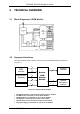
AL7020S, AL7024S Designer’s Guide 2. TECHNICAL OVERVIEW 2.1 Block Diagramm of GSM Module 2.2 Supported Interfaces The major hardware signal interfaces of the DF Series SocketGSM Modem are illustrated in Figure 1-1. 5 TTL Serial interface External SIM (Optional) Leds 1 3 3 1 Socket GSM Modem Module 1 1 2 Antenna Interface Speaker Microphone Interface Figure 2-1. Interface Block Diagram • • • • • • The RS232 Interface is connected via eight pins to the module.
AL7020S, AL7024S Designer’s Guide 3. HARDWARE INTERFACE 3.1 Interface Signals The Socket Modem pin assignments with DTE serial TTL interface, SIM Card and Analog Interface are shown in Figure 3-1 and are listed in Table 3-1. 3.2 Signal Description The Socket Modem interface signals are described in Table 3-3. The digital electrical characteristics are listed in Table 3-4. The analog electrical characteristics are listed in Table 3-5. Doc. No.
AL7020S, AL7024S Designer’s Guide 1 2 NC NC SPKR AGND MIC VCC 64 63 62 61 POWER AUDIO Top View 24 25 26 27 28 29 30 31 32 SIM / LED INTERFACE RESET# NC DGND LED-GPRS SIMVCC GSM LED SIMDATA SIMRST SIMCLK DGND DTR# DCD# CTS# DSR# RI# TXD# RXD# RTS# 41 40 39 38 37 36 35 34 33 SERIAL TTL INTERFACE Notes: Pins 3-23 and 42-60 are not installed. Figure 3-1. SERIAL PINOUT Table 3-1.
AL7020S, AL7024S Designer’s Guide Table 3-2. Signal Descriptions Label I/O Type Signal Name/Description +5 VDC. A standard 5V +/- 5% - 1.5A power supply is strictly required to supply this module (5V Versions). Average current is 270mA (350mA @ PCL5). See also chapter 5.1.2 VCC PWR +3.-3 VDC. A standard 3.3V +/- 5% - 1A power supply is strictly required to supply this module (3V Versions). Average current is 270mA (350mA @ PCL5). See also chapter 5.1.
AL7020S, AL7024S Designer’s Guide Table 3-3. Signal Descriptions (Cont'd) Label I/O Type Signal Name/Description The Serial interface signals are TTL-level signals. ~RTSTTL IB ~RXDTTL OB ~TXDTTL IA Request To Send (TTL Active Low). ~RTS is used to condition the local modem for data transmission and, during half-duplex operation, to control the direction of data transmission. On a full-duplex channel, RTS OFF maintains the modem in a non-transmit mode.
AL7020S, AL7024S Designer’s Guide Table 3-3. Signal Descriptions (Cont'd) Label I/O Type Signal Name/Description LED driver lines are open-drain inverter-driven (74HCT05) lines with 1.5 KΩ, 1/10W pull-up resistors. GSM LED OG GSM activity LED. active low ! connect LED to 5V with resistor in series. GPRS LED OG GPRS activity LED. active low ! connect LED to 5V with resistor in series. Audio/Headset Interface MICV I(DA) Microphone Voice Input.
AL7020S, AL7024S Designer’s Guide Table 3-5. Digital Electrical Characteristics Parameter Symbol Min. Typ. Max. Input High Voltage pins 33,35,40 VIH 2 - 5.5 Vdc Input Low Voltage pins 33,35,40 VIL 0 - 0.8 Vdc Output High Voltage pins 34,36,37,38 VOH VCC-0.1V VCC - Vdc 3.8V @VCC=4.5V 4.2 - ILOAD = -4 mA Output High Voltage VCC=4.5V pin 39 VOH VCC-0.1 VCC - ILOAD= -50 uA 3.8V - - ILOAD = -8 mA Output Low Voltage pins 34,36,37,38 VOL - 0 0 0.1 0.
AL7020S, AL7024S Designer’s Guide Table 3-6. Absolute Maximum Ratings Parameter Supply Voltage Symbol Min. Static Discharge Voltage Vdc Storage Temperature Range - 5.25 3.45 V - +/- 2500 TA °C -20 -20 - +60 +70 TSTG °C - +85 ID mA Average @PCL5 Average @PCL10 Average Idle Supply Current GSM 1800 +7.0 VESD -40 Supply Current GSM 900 - Vdc 4.75 3.20 Operational Functional Test Condition +6.0 VDD @ 25°C Operating Temperature Range - VIN 5V Version 3V Version Units Vdc -0.
AL7020S, AL7024S Designer’s Guide 3.4 Antenna Interface (RF) The AL7020S has two models, one for North America Frequency bands (850/1900 MHz), and one for European Bands (900/1800 MHz). The following connection requirements apply for the AL7020S antenna: • The AL7020S is terminated with an MMCX connector, and with 50-ohm impedance in the relevant frequencies. • The AL7020S can be connected to any antenna with 50-ohm impedance in the relevant frequency bands.
AL7020S, AL7024S Designer’s Guide 3.4.2 Antenna Performance Recommendations Table 3.7 - Antenna Performance Recommendations GSM 850 GSM 900 DCS 1800 PCS 1900 Gain: Impedance: VSWR: Frequencies: TX 824 – 849 MHz RX 869 – 893 MHz TX 880 – 915 MHz RX 925 – 960 MHz TX 1710 – 1785 MHz RX 1805 – 1880 MHz TX 1850 - 1910 MHz RX 1930 – 1990 MHz 0 dBi (unity) gain or greater 50 Ohm Typical: 1.5:1 Worst case: 2.5:1 3.4.
AL7020S, AL7024S Designer’s Guide 3.5 Internal SIM Card Interface The AL7020S module has a built-in SIM card reader within the module itself (see figure 3.5). The SIM card is inserted into the slot provided on the side of the connectors (bottom side). The SIM Interface controls a 3V SIM card. This interface is fully compliant with GSM 11.11 recommendation concerning SIM functions. 3.5.
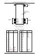
AL7020S, AL7024S Designer’s Guide 3.6 SIM Card Mechanical Drawings Doc. No.
AL7020S, AL7024S Designer’s Guide 3.7 External SIM Card Interface (-ES Option) 4 signals exist: • SIMVCC: SIM power supply. • SIMRST: reset. • SIMCLK: clock. • SIMDATA : I/O port. The SIM interface controls a 3V SIM. This interface is fully compliant with GSM 11.11 recommendations concerning SIM functions. It is recommended to add Transient Voltage Suppressor diodes on the signal connected to the SIM socket in order to prevent any Electrostatic Discharge.
AL7020S, AL7024S Designer’s Guide 3.7.3 SIM Card Reader Integration: SIM interface controls a 3V SIM only. We add Transient Voltage Suppressor (TVS) diodes with low capacitance (less than 10pF) on signal connected to the SIM socket in order to prevent any Electrostatic Discharge. They shall be placed as close as possible to the SIM socket. Following references are used: DALC208SC6 from ST Microelectronics, which will be connected, to SIMCLK and SIMDATA.
AL7020S, AL7024S Designer’s Guide 3.8 Audio - Interface 3.8.1 Speaker-Circuit Audio output is useful for monitoring the modem's call-progress tones and modem system debugging, as well as for fullfeatured Voice applications. You can directly connect a speaker of 32 to 150 Ohms to pins 63 and 64. The connection is singleended, with analog-ground at pin 63. Use good shielding of the audio-connections as to avoid disturbing performance by entering RF.
AL7020S, AL7024S Designer’s Guide 3.8.2 Microphone circuit The AL7020S has an analog input, referenced to the microphone ground (pin 63). The AL7020S contains an analog amplifier with a default gain of 22dB, which can be adjusted in seven steps between 0 and 31dB using the AT+MMICG command. For more details about this command, refer to the AT Commands document (AT_7020A). When the default gain of 22dB is used, then the level considerations should be as follows: Pin 62 is the headset microphone input.
AL7020S, AL7024S Designer’s Guide 3.9 Reset Signal (ON/OFF Signal) After power is applied to the AL7020S module, the power-on process is initiated, which lasts about five seconds, after which the module is ready to communicate. After power-on, the on/off signal is pulled high to the VCC by a 200kΩ resistor. The module remains active until power is turned off or the power-off process is initiated by activating the Reset (ON/OFF) signal.
AL7020S, AL7024S Designer’s Guide 4. CONNECTORS AND PERIPHERAL REFERENCE 4.1 RF CONNECTOR RF MMCX-connector and accessories can be obtained from • RADIALL (http://www.radiall.com/) • AMPHENOL (http://www.amphenol.com/) • HUBER&SUHNER (http://www.hubersuhner.com/) 4.2 Microphone Possible references : • HOSIDEN KUF3323 • HOSIDEN KUF4323 • PANASONIC WM64 4.3 Speaker Possible references : • SANYO M15X0080 • PHILIPS • PRIMO 4.
AL7020S, AL7024S Designer’s Guide 5. DESIGN GUIDELINES Good engineering practices must be adhered to when designing a printed circuit board (PCB) containing the GSM Socket Modem module. Suppression of noise is essential to the proper operation and performance of the modem itself and for surrounding equipment.
AL7020S, AL7024S Designer’s Guide 6. Locate cables and connectors so as to avoid coupling from high frequency circuits. 7. If a mulilayer board design is used, make no cuts in the ground or power planes and be sure the ground plane covers all traces. 8. Minimize the number of through-hole connections on traces carrying high frequency signals. 9. Avoid right angle turns on high frequency traces. Forty-five degree corners are good, however, radius turns are better 5.1.
AL7020S, AL7024S Designer’s Guide 5.1.3 Power Supply 3.3V (3V Models) A power supply with 3.3V +/- 5% (3V models) and a minimum power of 1A is strictly required to supply this module. The supply-regulator should be placed as close to the module as possible (about 5cm or nearer). To keep a short and low impedance connection between the regulator and the module is very important when supplying the module with 3.3V. The 3.3V-trace between regulator and module should be at least 2.
AL7020S, AL7024S Designer’s Guide 5.1.5 RF Antenna Antenna sub-system and integration in the application is a major issue. Attention should be paid to : • Choice of the antenna cable (type, length, performance, thermal resistance, etc) • Antenna connector (type + losses).
AL7020S, AL7024S Designer’s Guide 6. MODULE DIMENSIONS Top View 7.0 mm Top View Pin 1 2.0 FIGURE 6-2. MECHANICAL DRAWINGS Dimensions in Millimeters Doc. No.
AL7020S, AL7024S Designer’s Guide 7. REGULATORY APPROVALS The GSM Socket Modem is approved as a host-independent modem module. To maintain type approvals, permits and/or licenses valid, the guidelines described in this document must be followed. 7.1 Considerations for Regulatory Approvals The AL7020S Socket Modem has been assessed and has been found to comply with the following regulatory approvals: - FCC DOC PTCRB R&TTE EMC GCF 7.1.
AL7020S, AL7024S Designer’s Guide 7.2 Safety Precautions Your GSM terminal is based on the GSM standard for cellular technology. The GSM standard is spread all over the world. It covers Europe, Asia and some parts of America and Africa. This is the most used telecommunication standard. Your GSM terminal is actually a low power radio transmitter and receiver. It sends out and receives radio frequency energy.
AL7020S, AL7024S Designer’s Guide 8. APPENDIX A 8.1 REFERENCE DOCUMENTS GSM ETSI recommendations for Phase I and Phase II. Specification Reference Title GSM900/1800/1900 ph2 Radio ETSI GSM 05.05 v7.1.0 release 1998 GSM ph2 LinkManagement ETSI GSM 03.06, 04.08, 05.05, 05.08, 05.10, 07.01 and GT 01 v4.2.1 GSM ph2 Layer 2 ETSI GSM 04.06 and GT 01 v4.2.1 GSM900 ph2 Layer 3 ETSI GSM 04.08 and GT 01 v4.2.1 GSM1800 ph2 Layer 3 ETSI GSM 04.08 and GT 01 v4.2.1 GSM900/GSM1800 Multiband ETSI GSM 02.