Cyclone III 3C120 Development Board Reference Manual 101 Innovation Drive San Jose, CA 95134 www.altera.com Document Version: Document Date: 1.
Copyright © 2009 Altera Corporation. All rights reserved. Altera, The Programmable Solutions Company, the stylized Altera logo, specific device designations, and all other words and logos that are identified as trademarks and/or service marks are, unless noted otherwise, the trademarks and service marks of Altera Corporation in the U.S. and other countries. All other product or service names are the property of their respective holders. Altera products are protected under numerous U.S.
Contents Chapter 1. Overview Introduction . . . . . . . . . . . . . . . . . . . . . . . . . . . . . . . . . . . . . . . . . . . . . . . . . . . . . . . . . . . . . . . . . . . . . . . . . . . . General Description . . . . . . . . . . . . . . . . . . . . . . . . . . . . . . . . . . . . . . . . . . . . . . . . . . . . . . . . . . . . . . . . . . . . . Board Component Blocks . . . . . . . . . . . . . . . . . . . . . . . . . . . . . . . . . . . . . . . . . . . . . . . . . . . . . . . . . . . . . .
iv Communication Ports and Interfaces . . . . . . . . . . . . . . . . . . . . . . . . . . . . . . . . . . . . . . . . . . . . . . . . . . . . . . 2–37 USB 2.0 MAC/PHY . . . . . . . . . . . . . . . . . . . . . . . . . . . . . . . . . . . . . . . . . . . . . . . . . . . . . . . . . . . . . . . . . . 2–38 10/100/1000 Ethernet . . . . . . . . . . . . . . . . . . . . . . . . . . . . . . . . . . . . . . . . . . . . . . . . . . . . . . . . . . . . . . . . 2–40 High-Speed Mezzanine Connector . . . . . . . . . . .
1. Overview Introduction This document describes the hardware features of the Cyclone® III development board, including detailed pin-out information to enable you to create custom FPGA designs that interface with all components of the board. f For information about setting up and powering up the Cyclone III development board and using the kit’s demo software, refer to the Cyclone III Development Kit User Guide.
1–2 Chapter 1: Overview General Description The Cyclone III development board has the following main features: ■ High logic density to implement more functions and features ■ Embedded memory for high-bandwidth applications ■ Expandable through two Altera High-Speed Mezzanine Connectors (HSMCs) ■ 256-MB of dual channel DDR2 SDRAM with a 72-bit data width ■ Supports high-speed external memory interfaces including dual-channel DDR SDRAM and low-power SRAM ■ Four user push-button switches ■ Eight
Chapter 1: Overview General Description 1–3 ■ ■ FPGA configuration circuitry ■ MAX II CPLD and flash passive serial configuration ■ On-board USB-Blaster™ circuitry using the Quartus II Programmer On-board clocking circuitry ■ ■ 50 MHz ■ 125 MHz 80 I/O, 6 clocks, SMBus, and JTAG ■ SMA connector for external clock input and output General user and configuration interfaces ■ ■ ■ © March 2009 ■ ■ ■ ■ Two clock oscillators to support Cyclone III device user logic LEDs/displays: ■ Eight
1–4 Chapter 1: Overview General Description ■ ■ 1 Power supply ■ 14 V – 20 V DC input ■ On-board power measurement circuitry ■ Up to 19.8 W per HSMC interface Mechanical ■ 6” × 8” board ■ Bench-top design The Cyclone III FPGA Development Kit ships with additional HSMC daughter card loopback and break-out headers for convenient testing of some of the HSMC signals.
Chapter 1: Overview Handling the Board 1–5 Handling the Board When handling the board, it is important to observe the following precaution: c © March 2009 Static Discharge Precaution: Without proper anti-static handling, the board can be damaged. Therefore, use anti-static handling precautions when touching the board.
1–6 Cyclone III 3C120 Development Board Reference Manual Chapter 1: Overview Handling the Board © March 2009 Altera Corporation
2. Board Components Introduction This chapter introduces all the important components on the Cyclone III development board. Figure 2–1 illustrates all component locations and Table 2–1 describes component features.
2–2 Chapter 2: Board Components Board Overview Figure 2–1.
Chapter 2: Board Components Board Overview 2–3 Table 2–1. Cyclone III Development Board (Part 2 of 3) Board Reference Type Description J5 Header Speaker header. D1, D3, D4 Ethernet PHY LEDs Green Ethernet PHY LEDs. Illuminate when Ethernet PHY is using the 10/100/1000 Mbps (D1, D3, D4) connection speeds. D6 Duplex Ethernet PHY LED Green Ethernet PHY LED. Illuminates when Ethernet PHY is both sending and receiving data. D5 Power LED Blue LED indicates when power is applied to the board.
2–4 Chapter 2: Board Components Featured FPGA (U20) Table 2–1. Cyclone III Development Board (Part 3 of 3) Board Reference Type Description U23 and U24 SRAM The SRAM devices connect to the MAX II device as well as the flash memory device. U11, U12, U13, U25, U26 DDR2 SDRAM Four ×16 devices and a single ×8 device. Components and Interfaces U6 USB device USB device that provides JTAG programming of on-board devices, including the Cyclone III device and flash memory device.
Chapter 2: Board Components Featured FPGA (U20) 2–5 Table 2–4 lists the Cyclone III EP3C120F780C7 device pin count. Table 2–4. Cyclone III Device Pin Count Function I/O Type I/O Count Special Pins Oscillators and SMAs 1.8-V CMOS 4 Three clock inputs, one output DDR2 1.8-V SSTL 148 Nine data strobe signal (DQS), 10 VREF Flash/SRAM/MAX 1.8-V CMOS 78 — Horizontal bank OCT calibration 1.8-V CMOS 4 2 Rup, 2 Rdn Vertical bank OCT calibration 2.
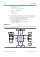
2–6 Chapter 2: Board Components MAX II CPLD Figure 2–2.
Chapter 2: Board Components MAX II CPLD 2–7 Figure 2–3. MAX II Device’s Block Diagram Power Display JTAG Header 2.5 V CMOS 2.5 V CMOS Power Measure To FPGA 64-MB Flash (x16) 2.5-V CMOS 1.8-V CMOS FSM Bus 8-MB SRAM (x32) FTDI 12 Mbps USB (x8) 24 MHz MAX II CPLD EPM2210GF256 PS Config 1.8-V CMOS MAX II Device Control DIP Switch 1.8-V CMOS JTAG Control DIP Switch 1.
2–8 Chapter 2: Board Components MAX II CPLD Table 2–5. MAX II Device Pin-Out (Note 1) (Part 2 of 8) MAX II Pin Number I/O Standard Signal Direction Schematic Signal Name M16 1.8 V Output FLASH_OEn L11 1.8 V Input FLASH_RDYBSYn M15 1.8 V Output FLASH_RESETn L12 1.8 V Output FLASH_WEn J16 1.8 V Input FPGA_BYPASS E3 2.5 V Input FPGA_CONF_DONE D3 2.5 V Output FPGA_DATA C2 2.5 V Output FPGA_DCLK N3 2.5 V Input FPGA_JTAG_TCK N1 2.5 V Output FPGA_JTAG_TDI N2 2.
Chapter 2: Board Components MAX II CPLD 2–9 Table 2–5. MAX II Device Pin-Out (Note 1) (Part 3 of 8) © March 2009 MAX II Pin Number I/O Standard Signal Direction Schematic Signal Name P4 1.8 V Bidirectional FSD[0] R1 1.8 V Bidirectional FSD[1] M6 1.8 V Bidirectional FSD[10] R5 1.8 V Bidirectional FSD[11] P7 1.8 V Bidirectional FSD[12] T5 1.8 V Bidirectional FSD[13] N7 1.8 V Bidirectional FSD[14] R6 1.8 V Bidirectional FSD[15] M7 1.8 V Bidirectional FSD[16] T6 1.
2–10 Chapter 2: Board Components MAX II CPLD Table 2–5.
Chapter 2: Board Components MAX II CPLD 2–11 Table 2–5. MAX II Device Pin-Out (Note 1) (Part 5 of 8) © March 2009 MAX II Pin Number I/O Standard Signal Direction Schematic Signal Name K2 2.5 V Output MAX_USER K15 1.8 V Input MAX_WEn H12 1.8 V Input MAX2_CLK M1 2.5 V Input MAXGP_JTAG_TCK L4 2.5 V Output MAXGP_JTAG_TDI L5 2.5 V Input MAXGP_JTAG_TDO M2 2.5 V Input MAXGP_JTAG_TMS N13 1.8 V Input MWATTS_MAMPS H13 1.8 V Input PGM[0] H15 1.8 V Input PGM[1] H14 1.
2–12 Chapter 2: Board Components MAX II CPLD Table 2–5. MAX II Device Pin-Out (Note 1) (Part 6 of 8) MAX II Pin Number I/O Standard Signal Direction Schematic Signal Name G15 — — RESERVED_INPUT K12 — — RESERVED_INPUT L13 — — RESERVED_INPUT P13 — — RESERVED_INPUT R16 — Input RESET_CONFIGn F16 — Output SRAM_ACTIVE F15 — Input SRAM_CSn B3 2.5 V Input USB_CLKOUT E10 2.5 V Input USB_CMD_DATA B10 2.5 V Output USB_EMPTY E9 2.5 V Bidirectional USB_FD[0] A9 2.
Chapter 2: Board Components MAX II CPLD 2–13 Table 2–5. MAX II Device Pin-Out (Note 1) (Part 7 of 8) © March 2009 MAX II Pin Number I/O Standard Signal Direction Schematic Signal Name A15 2.5 V Bidirectional USB_PHY_FD[3] D12 2.5 V Bidirectional USB_PHY_FD[4] B14 2.5 V Bidirectional USB_PHY_FD[5] C11 2.5 V Bidirectional USB_PHY_FD[6] B13 2.5 V Bidirectional USB_PHY_FD[7] D11 2.5 V Bidirectional USB_PHY_FD[8] A13 2.5 V Bidirectional USB_PHY_FD[9] C4 2.
2–14 Chapter 2: Board Components Configuration, Status, and Setup Elements Table 2–5. MAX II Device Pin-Out (Note 1) (Part 8 of 8) MAX II Pin Number I/O Standard Signal Direction Schematic Signal Name C16 — Power VCCIO3 H11 — Power VCCIO3 J11 — Power VCCIO3 P16 — Power VCCIO3 L8 — Power VCCIO4 L9 — Power VCCIO4 T3 — Power VCCIO4 T14 — Power VCCIO4 P15 1.
Chapter 2: Board Components Configuration, Status, and Setup Elements 2–15 Configuration This section discusses FPGA, flash memory, and MAX II device programming methods supported by the Cyclone III development board. FPGA Programming Over USB The FPGA can be configured at any time the board is powered on by using the USB 2.0 interface and the Quartus II Programmer in JTAG mode. The JTAG chain is mastered by the embedded USB Blaster function found in the MAX II device.
2–16 Chapter 2: Board Components Configuration, Status, and Setup Elements Table 2–7. JTAG Settings (Note 1) Number Description FPGA HSMA Bypass Bypass (SW3.1) (SW3.2) HSMB Bypass (SW3.3) MAX Enable (SW3.4) PFL Enable (SW1.
Chapter 2: Board Components Configuration, Status, and Setup Elements 2–17 Flash Programming over USB Interface The flash memory can be programmed at any time the board is powered up by using the USB 2.0 interface and the Quartus II Programmer ’s JTAG mode. The development kit implements the Altera PFL megafunction for flash programming. The PFL is a block of logic that is programmed into an Altera programmable logic device (FPGA or CPLD).
2–18 Chapter 2: Board Components Configuration, Status, and Setup Elements Table 2–8. Board-Specific LEDs (Part 2 of 2) Board Reference LED Name Description D1 10 MB Illuminates when Ethernet PHY is using the 10 Mbps connection speed. Driven by the Marvell 88E1111 PHY. D3 100 MB Illuminates when Ethernet PHY is using the 100 Mbps connection speed. Driven by the Marvell 88E1111 PHY. D4 1000 M Illuminates when Ethernet PHY is using the 1000 Mbps connection speed.
Chapter 2: Board Components Configuration, Status, and Setup Elements 2–19 ■ POWER SELECT rotary switch ■ PGM CONFIG SELECT rotary switch ■ Speaker header JTAG Control DIP Switch Board reference SW3 is a 4-position JTAG control DIP switch, and it is provided to either remove or include devices in the active JTAG chain. Additionally, JTAG control DIP switch is also used to disable the embedded USB-Blaster cable when using an external USB-Blaster cable (Table 2–10). Table 2–10.
2–20 Chapter 2: Board Components Configuration, Status, and Setup Elements MAX II Device Control DIP Switch Board reference SW1 is the board settings DIP switch, which controls various features specific to the Cyclone III development board and factory default (board test system) FPGA design: On = logic 0 and Off = logic 1. Table 2–12 lists the switch position, name, and description. Table 2–12.
Chapter 2: Board Components Configuration, Status, and Setup Elements 2–21 Table 2–14. Push Button Switch Signal Name and Function Description I/O Standard Schematic Signal Name Cyclone III Device Pin Number MAX II Device Pin Number S7 User defined push button 1.8 V FACTORY_CONFIG — A10 S6 User defined push button 1.8 V RESET_CONFIGn — R16 S5 User defined push button 1.
2–22 Chapter 2: Board Components Configuration, Status, and Setup Elements Table 2–16. Power Select Rotary Switch Number, Name, Pin, and Description (Part 2 of 2) Schematic Signal Name Number C — 12V D Power Pin Name — Description All 12-V power (voltage only) (1) — — E — — — F — — — Note to Table 2–16: (1) Display shows resistor divider output, not actual voltage as the A/D cannot take in sources higher than 3.0 V. See schematic page 5 for resistor dividers.
Chapter 2: Board Components Clocking Circuitry 2–23 Clocking Circuitry This section describes Cyclone III FPGA clocking inputs and outputs. A diagram is provided for each section. Cyclone III FPGA Clock Inputs Figure 2–5 outlines the clocking inputs to the Cyclone III FPGA. 1 Some signals are connected to 1.8-V banks and some are connected to 2.5-V banks. Refer to the Cyclone III Device Handbook for information about allowable levels for driving these inputs from external sources.
2–24 Chapter 2: Board Components Clocking Circuitry Cyclone III FPGA Clock Outputs Figure 2–6 outlines the clocking outputs from the Cyclone III FPGA. 1 Some signals are connected to 1.8-V banks and some are connected to 2.5-V banks. Refer to the Cyclone III Device Handbook for information about voltage output levels. The clock 1 and clock 2 signals from the HSMC interface can be used as LVDS pairs or as eight separate clock signals.
Chapter 2: Board Components Clocking Circuitry 2–25 Table 2–20. Cyclone III Development Board Clocking Parts List Board Reference Description Manufacturer Part Number Manufacturer Manufacturer Website Y5 50-MHz LVDS oscillator Pletronics SM5545TEX-50.00M www.pletronics.com Y4 125-MHz LVDS oscillator Pletronics SM5545TEX-125.00M www.pletronics.com J10, J11 SMA for external clock input/output Lighthorse Technologies LTI-SASF546-P26-X1 www.rfconnector.
2–26 Chapter 2: Board Components General User Interfaces General User Interfaces To allow you to fully leverage the I/O capabilities of the Cyclone III device for debugging, control, and monitoring purposes, the following general user interfaces are available on the board: ■ Push buttons ■ DIP switches ■ LEDs ■ 7-segment displays ■ LCD displays User-Defined Push Button Switches The development board includes four general user, one user reset, one system reset, and one factory push button switch.
Chapter 2: Board Components General User Interfaces 2–27 User-Defined DIP Switches Board reference SW6 is an 8-pin DIP switch. The switches in SW6 are user-defined, and are provided for additional FPGA input control. Each pin can be set to a logic 1 by pushing it to the open position, and each pin can be set to a logic 0 by pushing it to the closed position. There is no board-specific function for these switches.
2–28 Chapter 2: Board Components General User Interfaces Table 2–27. LED Reference Number, Schematic Signal Name, and Cyclone III Device Pin Number LED Board Reference Description I/O Standard Schematic Signal Name Cyclone III Device Pin Number D26 User-defined LED 1.8 V USER_LED7 AF19 D27 User-defined LED 1.8 V USER_LED6 AG19 D28 User-defined LED 1.8 V USER_LED5 AC17 D29 User-defined LED 1.8 V USER_LED4 AE15 D30 User-defined LED 1.8 V USER_LED3 AD19 D31 User-defined LED 1.
Chapter 2: Board Components General User Interfaces 2–29 Table 2–30. HSMC User-Defined LED Component Reference and Manufacturing Information Description Manufacturer Manufacturing Part Number Manufacturer Website Green LED, 1206, SMT, clear lens, 2.1 V Lumex, Inc. SML-LX1206GC-TR www.lumex.com Board Reference D12-D15 DDR2 User-Defined LEDs Each channel of DDR2 memory has an LED near the respective DDR2 device.
2–30 Chapter 2: Board Components General User Interfaces 7-Segment Displays This section discusses the following two on-board displays: ■ User 7-segment display ■ Power 7-segment display User 7-Segment Display Board reference U30 is a four-digit, user-defined, 7-segment display that is labeled User Display. Each segment’s LED driver input signals are multiplexed to each of the four digits and a minus sign.
Chapter 2: Board Components General User Interfaces 1 2–31 The four-pin, 7-segment display uses fewer pins than 2-digit, 7-segment displays. See Figure 2–7. Figure 2–7. 7-Segment Display 1 10 4 8 QUAD_7SEG_M2212R1 U30 DIGIT1 DIGIT2 DIGIT3 DIGIT4 A F B G E C DP DP 5 G 7 F 9 E 2 C D 8 3 B A 11 12 ca 13 14 an D Table 2–34 lists the 7-segment display component reference and manufacturing information. Table 2–34.
2–32 Chapter 2: Board Components General User Interfaces Character LCD (J4) The board contains a single 14-pin 0.1” pitch dual-row header, used to interface to a 16-character by 2-line LCD display, Lumex (part number LCM-S01602DSR/C). The LCD has a 14-pin receptacle that mounts directly to the board’s 14-pin header, so it can be easily removed for access to components under the display—or to use the header for debugging or other purposes. Table 2–36 summarizes the character LCD interface pins.
Chapter 2: Board Components General User Interfaces 1 2–33 The particular model used does not have a backlight and the LCD drive pin is not connected. Figure 2–8. LCD Display Block Diagram Block Diagram 16 X 2, 1/16 Duty, 1/5 Bias DB[7:0] E R/W RS Vss VDD Vo LCD Controller LSI and Driver SEC 80 COM 16 A K LCD Panel LED Backlight Table 2–38 lists the character LCD display component reference and manufacturing information. Table 2–38.
2–34 Chapter 2: Board Components General User Interfaces Table 2–39. Graphics LCD Interface I/O Board Reference Description I/O Standard Schematic Signal Name Cyclone III Device Pin Number J13 pin 6 LCD data bus bit 0 2.5 V LCD_DATA0 AA4 J13 pin 7 LCD data bus bit 1 2.5 V LCD_DATA1 AD1 J13 pin 8 LCD data bus bit 2 2.5 V LCD_DATA2 V8 J13 pin 9 LCD data bus bit 3 2.5 V LCD_DATA3 AB5 J13 pin 10 LCD data bus bit 4 2.5 V LCD_DATA4 AE2 J13 pin 11 LCD data bus bit 5 2.
Chapter 2: Board Components General User Interfaces 2–35 Table 2–40 is an excerpt from the OPTREX data sheet showing pin definitions for both serial and parallel interfaces. The included display has a parallel interface. Table 2–40.
2–36 Chapter 2: Board Components General User Interfaces Figure 2–9 is an excerpt from the OPTREX data sheet showing the control chip in the LCD module. The control chip is from New Japan Radio Corporation (part number NJU6676), and Figure 2–9 illustrates the functional block diagram of the display driver. f For more information, contact Optrex American at www.optrex.com or New Japan Radio at www.njr.co.jp/index_e.htm. Figure 2–9.
Chapter 2: Board Components Communication Ports and Interfaces 2–37 Figure 2–10 is an excerpt from the Optrex data sheet and shows the module interface signals for both read and write transactions. Figure 2–10. Graphics LCD Timing Diagram t CYC8 A0, CS1 t AW8 t WR, RD t AH8 t CCH(W/R) CCL(W/R) t DS8 D0~D7 (Write) tf t DH8 tr t ACC8 t OH8 D0~D7 (Read) f For more information about timing parameters, visit www.optrex.com.
2–38 Chapter 2: Board Components Communication Ports and Interfaces USB 2.0 MAC/PHY The board incorporates the FTDI USB 2.0 PHY chip. The FT245BL (LQFP package) provides an easy cost-effective method of transferring data to/from a peripheral and a host PC at up to 8 million bits (1 Megabyte) per second (Mbps). The simple, FIFO-like design makes interfacing easier. The device interfaces to J3, a Type B USB connector similar to those used by common peripherals such as digital cameras and printers.
Chapter 2: Board Components Communication Ports and Interfaces 2–39 Table 2–42 lists the FTDI USB interface pins. Signal name and direction are relative to the MAX II CPLD. Table 2–42. FTDI USB PHY Interface I/O Signal Names Description Type USB_FD(7:0) FIFO data bus 2.5-V CMOS in/out (8 bit) (1) USB_RDn FIFO data bus read enable 2.5-V CMOS in (1) USB_WR FIFO data bus write enable 2.5-V CMOS in (1) USB_RXFn FIFO data bus RX enable 2.5-V CMOS out (1) USB_TXEn FIFO data bus TX enable 2.
2–40 Chapter 2: Board Components Communication Ports and Interfaces 10/100/1000 Ethernet The 10/100/1000 Ethernet PHY port is provided using a dedicated 10/100/1000 base-T, auto-negotiating Ethernet PHY with reduced Gigabit media independent interface (RGMII) to the FPGA. The target device is the Marvell 88E1111, which uses 2.5-V and 1.2-V power rails. The Marvell 88E1111 requires a 25-MHz reference clock driven from a dedicated oscillator.
Chapter 2: Board Components Communication Ports and Interfaces 2–41 Table 2–44. Ethernet PHY Interface I/O (Part 2 of 2) Board Reference Cyclone III Device Pin Number Description I/O Standard Schematic Signal Name U5 pin 12 RGMII interface transmit data bus bit 1 2.5 V ENET_TX_D1 AA5 U5 pin 14 RGMII interface transmit data bus bit 2 2.5 V ENET_TX_D2 Y5 U5 pin 16 RGMII interface transmit data bus bit 3 2.5 V ENET_TX_D3 W3 U5 pin 9 RGMII interface transmit control 2.
2–42 Chapter 2: Board Components Communication Ports and Interfaces High-Speed Mezzanine Connector The board contains two HSMC interfaces called Port A and Port B. These HSMC interfaces support both single-ended and differential signaling. The connector part number is Samtec ASP-122953-01. The HSM connector interface also allows for JTAG, SMBus, clock outputs and inputs, as well as power for compatible HSMC daughter cards.
Chapter 2: Board Components Communication Ports and Interfaces 1 2–43 As noted in the HSMC specification, LVDS and single-ended I/O standards are only guaranteed to function when mixed according to either the generic single-ended pin-out or the generic differential pin-out. Table 2–47 lists the HSMC Port A interface signal name, description, and I/O standard. Signal name and direction are relative to the Cyclone III FPGA, which is the HSMC host. Table 2–47.
2–44 Chapter 2: Board Components Communication Ports and Interfaces Table 2–47. HSMC Port A Interface Signal Name, Description, and Type (Part 2 of 3) Board Reference Description I/O Standard Schematic Signal Name Cyclone III Device Pin Number J8 pin 79 LVDS TX 5n or CMOS I/O data bit 26 LVDS or 2.5 V HSMA_TX_D_N5 P1 J8 pin 80 LVDS RX 5n or CMOS I/O data bit 27 LVDS or 2.5 V HSMA_RX_D_N5 U1 J8 pin 83 LVDS TX 6p or CMOS I/O data bit 28 LVDS or 2.
Chapter 2: Board Components Communication Ports and Interfaces 2–45 Table 2–47. HSMC Port A Interface Signal Name, Description, and Type (Part 3 of 3) Board Reference Description I/O Standard Schematic Signal Name Cyclone III Device Pin Number J8 pin 137 LVDS TX 14p or CMOS I/O data bit 64 LVDS or 2.5 V HSMA_TX_D_P14 F5 J8 pin 138 LVDS TX 14p or CMOS I/O data bit 65 LVDS or 2.5 V HSMA_RX_D_P14 G4 J8 pin 139 LVDS RX 14n or CMOS I/O data bit 66 LVDS or 2.
2–46 Chapter 2: Board Components Communication Ports and Interfaces Table 2–48. HSMC Port B Interface Signal Name, Description, and Type (Part 2 of 4) Board Reference Description I/O Standard Schematic Signal Name Cyclone III Device Pin Number J9 pin 49 LVDS TX 0n or CMOS I/O data bit 6 LVDS or 2.5 V HSMB_TX_D_N0 J26 J9 pin 50 LVDS RX 0n or CMOS I/O data bit 7 LVDS or 2.5 V HSMB_RX_D_N0 F28 J9 pin 53 LVDS TX 1p or CMOS I/O data bit 8 LVDS or 2.
Chapter 2: Board Components Communication Ports and Interfaces 2–47 Table 2–48. HSMC Port B Interface Signal Name, Description, and Type (Part 3 of 4) Board Reference Description I/O Standard Schematic Signal Name Cyclone III Device Pin Number J9 pin 107 LVDS TX 9p or CMOS I/O data bit 44 LVDS or 2.5 V HSMB_TX_D_P9 W25 J9 pin 108 LVDS RX 9p or CMOS I/O data bit 45 LVDS or 2.5 V HSMB_RX_D_P9 R22 J9 pin 109 LVDS TX 9n or CMOS I/O data bit 46 LVDS or 2.
2–48 Chapter 2: Board Components On-Board Memory Table 2–48. HSMC Port B Interface Signal Name, Description, and Type (Part 4 of 4) Board Reference Description I/O Standard Schematic Signal Name Cyclone III Device Pin Number N/A User LED intended to show RX data activity on the HSMC interface 2.5 V HSMB_RX_LED F26 N/A User LED intended to show TX data activity on the HSMC interface 2.5 V HSMB_TX_LED D28 The board provides both 12 V and 3.3 V to installed daughter cards up to 18.6 W each.
Chapter 2: Board Components On-Board Memory 2–49 The two address buses are large enough to support any size JEDEC-compliant DDR2 device, as they have all 16 address pins and all three bank pins connected. The Micron components shipped on the board all have 13 row addresses, 2 bank addresses, and 10 column addresses. 1 Unused control pins should be left tri-stated to reduce power consumption. There are three clock pairs driven from the FPGA to the memories.
2–50 Chapter 2: Board Components On-Board Memory Table 2–51.
Chapter 2: Board Components On-Board Memory 2–51 Table 2–51.
2–52 Chapter 2: Board Components On-Board Memory Table 2–51.
Chapter 2: Board Components On-Board Memory 2–53 Table 2–51.
2–54 Chapter 2: Board Components On-Board Memory SRAM The board features 8 MB of SRAM memory with a 32-bit data bus. The devices use 1.8-V CMOS signaling and are optimized for low cost and power. The 32-bit interface comprises two ×16 devices. The Samsung part features a maximum frequency of 104 MHz (104 Mbps). The theoretical bandwidth of the entire interface is 416 Mbps.
Chapter 2: Board Components On-Board Memory 2–55 Table 2–53. SRAM Interface I/O (Part 2 of 3) Board Reference Description Schematic Signal I/O Standard Name Cyclone III Device Pin Number U23, U24 pin G4 Address bit 14 (DWORD aligned) 1.8 V FSA14 AC22 U23, U24 pin F3 Address bit 15 (DWORD aligned) 1.8 V FSA15 AE8 U23, U24 pin F4 Address bit 16 (DWORD aligned) 1.8 V FSA16 AF13 U23, U24 pin E4 Address bit 17 (DWORD aligned) 1.
2–56 Chapter 2: Board Components On-Board Memory Table 2–53. SRAM Interface I/O (Part 3 of 3) Board Reference Cyclone III Device Pin Number Schematic Signal I/O Standard Name Description U24 pin F1 Data bit 30 1.8 V FSD30 H10 U24 pin G1 Data bit 31 1.8 V FSD31 J10 Figure 2–14 illustrates the latency for both fixed and variable modes of operation. For asynchronous accesses, each of the two devices has its own WAIT pin wired to the Cyclone III device.
Chapter 2: Board Components On-Board Memory 2–57 Figure 2–15 and Figure 2–16 show the Samsung device read and write access waveforms, respectively. Figure 2–15. SRAM Read Timing Waveforms 0 1 2 3 4 5 6 7 8 9 10 11 12 13 14 11 12 13 14 CLK ADV ADDR CS UB, LB OE Data Out WAIT Figure 2–16.
2–58 Chapter 2: Board Components On-Board Memory Table 2–55 lists the SRAM board reference and manufacturing information. Table 2–55. SRAM Manufacturing Information Board Reference U23, U24 f Description Manufacturer 32 MB (2 M × 16) of SRAM Samsung Semiconductor Manufacturer Part Number Manufacturer Website K1B3216B2E-BI70 www.samsung.com For more information about timing parameter values, mode register settings (MRS), or any other data regarding the Samsung device, visit www. samsung.com.
Chapter 2: Board Components On-Board Memory 2–59 Table 2–56. Flash Interface I/O (Part 2 of 2) Board Reference Description I/O Standard Schematic Signal Name Cyclone III Device Pin Number U31 pin C6 Address bus bit 10 (word aligned) 1.8 V FSA10 AH6 U31 pin D6 Address bus bit 11 (word aligned) 1.8 V FSA11 AD24 U31 pin B7 Address bus bit 12 (word aligned) 1.8 V FSA12 AF9 U31 pin A7 Address bus bit 13 (word aligned) 1.8 V FSA13 AA8 U31 pin C7 Address bus bit 14 (word aligned) 1.
2–60 Chapter 2: Board Components On-Board Memory Table 2–57 defines the flash memory map and lists the signals required for flash memory. Signal directions are relative to the Cyclone FPGA. Table 2–57. Flash Memory Map Defined Signal Name Description I/O Standard FSM_A(24:0) Address bus (word aligned) 1.8-V LVCMOS out (25 bits) FSM_D(15:0) Data bus N/A (Accounted for in SRAM section) FLASH_CSn Chip select 1.8-V LVCMOS out FLASH_OEn Output enable 1.8-V LVCMOS out FLASH_WEn Write enable 1.
Chapter 2: Board Components On-Board Memory 2–61 Table 2–58. Flash Memory Map (Part 2 of 2) Name Address FPGA Design 3 0x00DE.EBE1 0x00A8.0000 FPGA Design 2 0x00A6.EBE1 0x0070.0000 FPGA Design 1 0x006E.EBE1 0x0038.0000 FPGA Design 0 (factory design) 0x0036.EBE1 0x0000.0000 f For information about the flash array command set and sequencing for register access, or any other data regarding the Spansion device, visit www.spansion.com.
2–62 Chapter 2: Board Components Power Supply Power Supply The board’s power is provided through an IBM laptop style DC power input. The input voltage must be in the range of 14 V to 20 V. The DC voltage is then stepped down to the various power rails used by the components on the board and installed into the HSM connectors. Figure 2–17 shows the power distribution system, which uses current power rails as described in “POWER SELECT Rotary Switch” on page 2–21.
Chapter 2: Board Components Power Supply 2–63 Figure 2–17. Power Distribution System R Wide Input Switching Regulator (LT3481) MEASURE 1.2V 2.013A R 12V 0.013A Wide Input Switching Regulator (LTM4601) 12V PowerNet HMCA Port A HMCB Port B 12V 2.000A 5.0V 0.013A 3.3V Partial Plane Flash VDD, FTDI USB VCC, Cypress USB VCC/AVCC, 25M Oscillator, HSMC Port A, HSMC Port B R MEASURE 3.3V 4.169A 10.429A 3.3V 0.002A DC Input 14V - 20V 3.3V 1.036A Linear 80% eff. (LT1761) Linear (LT1963) 3.
2–64 Chapter 2: Board Components Statement of China-RoHS Compliance Power Measurement Eight power supply rails have on-board voltage and current sense capabilities. These measurements are made using an 8-channel differential A/D converter from Linear Technology, with a serial data bus connected to the MAX II CPLD. The MAX II CPLD contains a logic design that continually monitors the power rails and displays the current in mW on the dedicated four-digit 7-segment display.
Chapter 2: Board Components Statement of China-RoHS Compliance 2–65 Table 2–62.
2–66 Cyclone III 3C120 Development Board Reference Manual Chapter 2: Board Components Statement of China-RoHS Compliance © March 2009 Altera Corporation
Additional Information Revision History The following table displays the revision history for this reference manual. Date Version Changes Made March 2009 1.4 Updated Table 2–10 and Table 2–12. December 2008 1.3 Corrected “Schematic Signal Names” in Table 2–47 and Table 2–48. August 2008 1.2 ■ Corrected “Schematic Signal Names” in Table 2–5 and added (Note 1). ■ Updated JTAG settings in Table 2–7. ■ Updated Table 2–16.
Info–2 Additional Information How to Contact Altera How to Contact Altera For the most up-to-date information about Altera products, refer to the following table. Contact (Note 1) Contact Method Address Technical support Website www.altera.com/support Technical training Website www.altera.com/training Email custrain@altera.com Website www.altera.com/literature Product literature Non-technical support (General) Email (Software Licensing) Email nacomp@altera.com authorization@altera.
Additional Information Typographic Conventions Visual Cue Info–3 Meaning c A caution calls attention to a condition or possible situation that can damage or destroy the product or your work. w A warning calls attention to a condition or possible situation that can cause you injury. r The angled arrow instructs you to press Enter. f The feet direct you to more information about a particular topic.
Info–4 Cyclone III 3C120 Development Board Reference Manual Additional Information Typographic Conventions © March 2009 Altera Corporation