
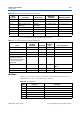
Specifications

Chapter 2: Board Components 2–23
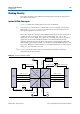
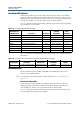
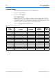
Clocking Circuitry
© March 2009 Altera Corporation Cyclone III 3C120 Development Board Reference Manual
Clocking Circuitry
This section describes Cyclone III FPGA clocking inputs and outputs. A diagram is
provided for each section.
Cyclone III FPGA Clock Inputs
Figure 2–5 outlines the clocking inputs to the Cyclone III FPGA.
1 Some signals are connected to 1.8-V banks and some are connected to 2.5-V banks.
Refer to the Cyclone III Device Handbook for information about allowable levels for
driving these inputs from external sources.
The clock 1 and clock 2 signals from the HSMC interface can be used as LVDS pairs or
as eight separate clock signals. These signals include HSMA_CLK_IN_P2/N2,
HSMA_CLK_IN_P1/N1, HSMB_CLK_IN_P2/N2, and HSMB_CLK_IN_P1/N1. These
signals may also be used for bidirectional data. If used in LVDS mode, install
applicable termination resistors between P/N pairs. A voltage translator, National
Semiconductor part number FXLP34, is located in between the HSMC interfaces and
the Cyclone III FPGA to reduce LVTTL to 1.8-V CMOS input levels for clock 0 signals
HSMA_CLK_IN0 and HSMB_CLK_IN0.
f For more information, refer to the Cyclone III development board schematics
included in the development kit.
Figure 2–5. Cyclone III FPGA Clock Inputs
Bank 8
1.8 V
Bank 7
1.8 V
Bank 3
1.8 V
Bank 4
1.8 V
Bank 6
2.5 V
Bank 5
2.5 V
Bank 1
2.5 V
Bank 2
2.5 V
HSMC
Port A
ENET
PHY
HSMA_CLK_IN_P2
HSMA_CLK_IN_N2
HSMA_CLK_IN_P1
HSMA_CLK_IN_N1
HSMA_CONN_CLK_IN0
HSMA_CLK_IN0
HSMC
Port B
HSMB_CLK_IN_P1
HSMB_CLK_IN_N1
HSMA_CLK_IN_P2
HSMA_CLK_IN_N2
ENET_RX_CLK
CLKIN_SMA
CLKIN_50
MAX II CPLD
BUF
SMA Input 50 MHz
CLKIN_125
USB_IFCLK
125 MHz
3.3V 1.8V
HSMB_CLK_IN0
HSMB_CONN_CLK_IN0
BUF
3.3 V1.8 V
CLK0
CLK1
CLK2
CLK3
CLK4
CLK8 CLK9 CLK10 CLK11
CLK12
CLK13
CLK14
CLK5
CLK6
CLK7
CLK15