
Specifications

2–40 Chapter 2: Board Components
Communication Ports and Interfaces
Cyclone III 3C120 Development Board Reference Manual © March 2009 Altera Corporation
10/100/1000 Ethernet
The 10/100/1000 Ethernet PHY port is provided using a dedicated 10/100/1000
base-T, auto-negotiating Ethernet PHY with reduced Gigabit media independent
interface (RGMII) to the FPGA. The target device is the Marvell 88E1111, which uses
2.5-V and 1.2-V power rails. The Marvell 88E1111 requires a 25-MHz reference clock
driven from a dedicated oscillator.
The Marvell device is provided for copper RS-45 Ethernet connectivity and comes in
the BCC96 leadless chip carrier package. The device interfaces to a HALO
HFJ11-1G02E model RJ-45.
The PHY device provides 32 internal management registers that can be accessed using
the Management Interface (MDIO). The MDIO address of the PHY device is
configured to the value 18 (0x12).
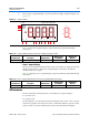
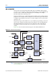
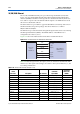
Figure 2–12 shows the interface between the FPGA and the PHY device.
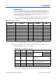
Ta bl e 2–44 lists the signal name, description, and I/O standard for the Ethernet PHY
interface I/O. The signal name and type are relative to the Cyclone III device, i.e., the
I/O setting and direction.
Figure 2–12. Interface Between the FPGA and the PHY Device
TXC
TX_EN
TD[3:0]
GTX_CLK
TX_EN
TDX[3:0]
RXC
RX_DV
RD[3:0]
RX_CLK
RX_DV
RXD[3:0]
Cyclone III
Device
MAC Block
Marvell 88E111
RGMII Interface
PHY Layer
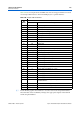
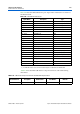
Table 2–44. Ethernet PHY Interface I/O (Part 1 of 2)
Board
Reference Description I/O Standard
Schematic
Signal Name
Cyclone III
Device Pin
Number
U5 pin 8 RGMII interface transmit clock 2.5 V ENET_GTX_CLK T8
U5 pin 73 1000 MB link established 2.5 V ENET_LED_LINK1000 AC25
U5 pin 25 Management bus data clock 2.5 V ENET_MDC N8
U5 pin 24 Management bus data 2.5 V ENET_MDIO L5
U5 pin 28 Reset 2.5 V ENET_RESETN AD2
U5 pin 2 RGMII interface receive clock 1.8 V ENET_RX_CLK B14
U5 pin 95 RGMII interface receive data bus bit 0 2.5 V ENET_RX_D0 W8
U5 pin 92 RGMII interface receive data bus bit 1 2.5 V ENET_RX_D1 AA6
U5 pin 93 RGMII interface receive data bus bit 2 2.5 V ENET_RX_D2 W7
U5 pin 91 RGMII interface receive data bus bit 3 2.5 V ENET_RX_D3 Y6
U5 pin 94 RGMII interface receive control 2.5 V ENET_RX_DV AB4
U5 pin 11 RGMII interface transmit data bus bit 0 2.5 V ENET_TX_D0 W4