
User guide

6–4 Chapter 6: Board Test System
Using the Board Test System
Cyclone III FPGA Development Kit User Guide September 2010 Altera Corporation
Using the Board Test System
This section describes each control in the Board Test System application.
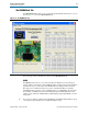
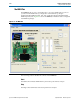
The Configure Menu
Each test design tests different functionality and corresponds to one or more
application tabs. Use the Configure menu to select the design you want to use.
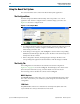
Figure 6–2 shows the Configure menu.
1. To configure the FPGA with a test system design, perform the following steps:On
the Configure menu, click the configure command that corresponds to the
functionality you wish to test.
2. In the dialog box that appears, click Configure to download the corresponding
SRAM/Flash/GPIO design object file (.sof) to the FPGA. The download process
usually takes about a minute.
3. When configuration finishes, the design begins running in the FPGA. The
corresponding GUI application tab that interfaces with the design is enabled.
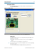
The Config Tab
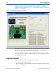
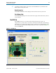
The Config tab shows information about the board’s current configuration.
Figure 6–1 on page 6–2 shows the Config tab. The tab displays the contents of the
JTAG chain, the flash memory map, and other details stored on the board.
The following sections describe the controls on the Config tab.
MAX II Registers
The MAX II registers control allow you to view the current MAX II register values.
The values are set when you load the test system design into the FPGA and is not
configurable.
JTAG Chain
The JTAG chain control shows all the devices currently in the JTAG chain. The
Cyclone III device is always the first device in the chain.
Figure 6–2. The Configure Menu