
User guide


7–4 Chapter 7: Power Measurement
Measuring Power
Cyclone III FPGA Development Kit User Guide September 2010 Altera Corporation
2. Download the cycloneIII_dev_powerdemo.sof file as described in “Configuring
the FPGA” on page 4–4. The power design example is in
<path>\...\examples\cycloneIII_3c120_dev_powerdemo.
3. Set the POWER SELECT rotary switch SW4 to 5.
4. Observe the 4-digit hexadecimal display for the I/O output power in watts on
banks 1 and 2.
5. Using the user input push buttons (Table 7–1 on page 7–1), advance through the
power states in Table 7–2 and Table 7–3 on page 7–2. Notice how power increases
as frequency and resources increase.
6. Press the User_PB3 button to enable the output pins on the HSMC connectors J8
and J9. LED7 (AF19), signal
o_noutput_ena_state
, lights to indicate that the
outputs are enabled and toggling. Enabling the outputs further increases power
for each resource utilization percentage used by the Cyclone III FPGA.
7. Press the User_PB3 button again to disable the outputs. LED7 turns off.
8. Set the POWER SELECT rotary switch SW4 to 6.
9. Repeat steps 4 through 7 to observe the I/O output power in watts on banks 5 and
6.
The sum of power results from the two sets of I/O banks provides the total FPGA I/O
power.
f For specific information about on-board measurements and the POWER SELECT
rotary switch, refer to the Cyclone III 3C120 Development Board Reference Manual.
Measuring Voltage with a DMM
To obtain power values by using a DMM, measure voltage across the sense resistors,
R49, R48, and R51 on the board, then use the voltage measurements to calculate
power.
1 For best results, use a DMM with six-digit for greater accuracy.
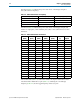
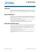
FPGA I/O power is distributed by banks (Table 7–5), for which the sense resistors are
components R48 and R51. For the I/O power calculation, use the sum of voltage
measurements across these resistors while outputs are enabled. For the FPGA core
power calculation, measure the sense resistor voltage across R49.
Table 7–5. Sense Resistors
FPGA Power Voltage
Sense
Resistor
Resistor
Value
I/O
Banks 1 and 2 2.5 V R48 0.009 Ω
Banks 5 and 6 2.5 V R51 0.009 Ω
Core: V
CC_INT
1.2 V R49 0.009 Ω