Altera DE2-70 Board Version 1.
Altera DE2 Board CONTENTS Chapter 1 DE2-70 Package ...............................................................................................................1 1.1 1.2 1.3 Package Contents .................................................................................................................1 The DE2-70 Board Assembly ..............................................................................................2 Getting Help....................................................................
Altera DE2 Board 5.12 5.13 5.14 5.15 5.16 TV Decoder........................................................................................................................52 Implementing a TV Encoder..............................................................................................54 Using USB Host and Device..............................................................................................55 Using IrDA..................................................................................
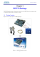
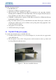
DE2-70 User Manual Chapter 1 DE2-70 Package The DE2-70 package contains all components needed to use the DE2-70 board in conjunction with a computer that runs the Microsoft Windows software. 1.1 Package Contents Figure 1.1 shows a photograph of the DE2-70 package. Figure 1.1. The DE2-70 package contents.
DE2-70 User Manual The DE2-70 package includes: • • • The DE2-70 board USB Cable for FPGA programming and control DE2-70 System CD containing the DE2-70 documentation and supporting materials, including the User Manual, the Control Panel utility, reference designs and demonstrations, device datasheets, tutorials, and a set of laboratory exercises • CD-ROMs containing Altera’s Quartus® II Web Edition and the Nios® II Embedded Design Suit Evaluation Edition software.
DE2-70 User Manual 1.3 Getting Help Here are the addresses where you can get help if you encounter problems: • Altera Corporation 101 Innovation Drive San Jose, California, 95134 USA Email: university@altera.com • Terasic Technologies No. 356, Sec. 1, Fusing E. Rd. Jhubei City, HsinChu County, Taiwan, 302 Email: support@terasic.com Web: DE2-70.terasic.
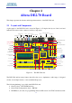
DE2-70 User Manual Chapter 2 Altera DE2-70 Board This chapter presents the features and design characteristics of the DE2-70 board. 2.1 Layout and Components A photograph of the DE2-70 board is shown in Figure 2.1. It depicts the layout of the board and indicates the location of the connectors and key components.
DE2-70 User Manual (AS) programming modes are supported • • • • • • • • • • • • • • • • • • • 2-Mbyte SSRAM Two 32-Mbyte SDRAM 8-Mbyte Flash memory SD Card socket 4 pushbutton switches 18 toggle switches 18 red user LEDs 9 green user LEDs 50-MHz oscillator and 28.
DE2-70 User Manual Figure 2.2. Block diagram of the DE2-70 board. Following is more detailed information about the blocks in Figure 2.
DE2-70 User Manual SSRAM • • • 2-Mbyte standard synchronous SRAM Organized as 512K x 36 bits Accessible as memory for the Nios II processor and by the DE2-70 Control Panel SDRAM • • • Two 32-Mbyte Single Data Rate Synchronous Dynamic RAM memory chips Organized as 4M x 16 bits x 4 banks Accessible as memory for the Nios II processor and by the DE2-70 Control Panel Flash memory • • • 8-Mbyte NOR Flash memory Support both byte and word mode access Accessible as memory for the Nios II processor and by the
DE2-70 User Manual Audio CODEC • • • • Wolfson WM8731 24-bit sigma-delta audio CODEC Line-level input, line-level output, and microphone input jacks Sampling frequency: 8 to 96 KHz Applications for MP3 players and recorders, PDAs, smart phones, voice recorders, etc.
DE2-70 User Manual Serial ports • • • • One RS-232 port One PS/2 port DB-9 serial connector for the RS-232 port PS/2 connector for connecting a PS2 mouse or keyboard to the DE2-70 board IrDA transceiver • • • • • Contains a 115.
DE2-70 User Manual At this point you should observe the following: • • • • • • All user LEDs are flashing All 7-segment displays are cycling through the numbers 0 to F The LCD display shows Welcome to the Altera DE2-70 The VGA monitor displays the image shown in Figure 2.3.
DE2-70 User Manual Chapter 3 DE2-70 Control Panel The DE2-70 board comes with a Control Panel facility that allows users to access various components on the board from a host computer. The host computer communicates with the board through an USB connection. The facility can be used to verify the functionality of components on the board or be used as a debug tool while developing RTL code.
DE2-70 User Manual close that port; you cannot use Quartus II to download a configuration file into the FPGA until you close the USB port. 7. The Control Panel is now ready for use; experiment by setting the value of some LEDs display and observing the result on the DE2-70 board. Figure 3.1. The DE2-70 Control Panel. The concept of the DE2-70 Control Panel is illustrated in Figure 3.2. The “Control Codes” that performs the control functions is implemented in the FPGA board.
DE2-70 User Manual 7-SEG Display 16x2 LCD USB Blaster SDRAM Flash SSRAM Control Codes PS/2 USB Device SD Card Soket LEDs Figure 3.2. The DE2-70 Control Panel concept. The DE2-70 Control Panel can be used to light up LEDs, change the values displayed on 7-segment and LCD displays, monitor buttons/switches status, read/write the SDRAM, SSRAM and Flash Memory, monitor the status of an USB mouse, read data from a PS/2 keyboard, and read SD-CARD specification information.
DE2-70 User Manual Figure 3.3. Controlling LEDs. Choosing the 7-SEG tab leads to the window in Figure 3.4. In the tab sheet, directly use the Up-Down control and Dot Check box to specified desired patterns, the 7-SEG patterns on the board will be updated immediately. Figure 3.4. Controlling 7-SEG display.
DE2-70 User Manual Choosing the LCD tab leads to the window in Figure 3.5. Text can be written to the LCD display by typing it in the LCD box and pressing the Set button. Figure 3.5. Controlling LEDs and the LCD display. The ability to set arbitrary values into simple display devices is not needed in typical design activities. However, it gives the user a simple mechanism for verifying that these devices are functioning correctly in case a malfunction is suspected.
DE2-70 User Manual Figure 3.6. Monitoring switches and buttons. The ability to check the status of button and switch is not needed in typical design activities. However, it provides users a simple mechanism for verifying if the buttons and switches are functioning correctly. Thus, it can be used for troubleshooting purposes. 3.4 SDRAM/SSRAM/Flash Controller and Programmer The Control Panel can be used to write/read data to/from the SDRAM, SSRAM, and FLASH chips on the DE2-70 board.
DE2-70 User Manual Figure 3.7. Accessing the SDRAM-U1. A 16-bit word can be written into the SDRAM by entering the address of the desired location, specifying the data to be written, and pressing the Write button. Contents of the location can be read by pressing the Read button. Figure 3.7 depicts the result of writing the hexadecimal value 06CA into location 200, followed by reading the same location.
DE2-70 User Manual into the memory. The Sequential Read function is used to read the contents of the SDRAM-U1 and place them into a file as follows: 1. Specify the starting address in the Address box. 2. Specify the number of bytes to be copied into the file in the Length box. If the entire contents of the SDRAM-U1 are to be copied (which involves all 32 Mbytes), then place a checkmark in the Entire Memory box. 3. Press Load Memory Content to a File button. 4.
DE2-70 User Manual Figure 3.8. USB Mouse Monitoring Tool. 3.6 PS2 Device The Control Panel provides users a tool to receive the inputs from a PS2 keyboard in real time. The received scan-codes are translated to ASCII code and displayed in the control window. Only visible ASCII codes are displayed. For control key, only “Carriage Return/ENTER” key is implemented. This function can be used to verify the functionality of the PS2 Interface. Please follow the steps below to exercise the PS2 device: 1.
DE2-70 User Manual Figure 3.9. Reading the PS2 Keyboard. 3.7 SD CARD The function is designed to read the identification and specification of the SD card. The 1-bit SD MODE is used to access the SD card. This function can be used to verify the functionality of SD-CARD Interface. Follow the steps below to exercise the SD card: 1. Choosing the SD-CARD tab leads to the window in Figure 3.10. First, 2. Insert a SD card to the DE2-70 board, then press the Read button to read the SD card.
DE2-70 User Manual Figure 3.10. Reading the SD card Identification and Specification. 3.8 Audio Playing and Recording This interesting audio tool is designed to control the audio chip on the DE2-70 board for audio playing and recording. It can play audio stored in a given WAVE file, record audio, and save the audio signal as a wave file. The WAVE file must be uncompressed, stereo (2 channels per sample), and 16-bits per channel. Its sample rate must be either 96K, 48K, 44.1K, 32K, or 8K.
DE2-70 User Manual Figure 3.11. Playing audio from a selected wave file To record sound using a microphone, please follow the steps below: 1. Plug a microphone to the MIC port on the board. 2. Select the “Record MIC” item in the com-box and select desired sampling rate, as shown in Figure 3.12. 3. Click “Start Record” to start the record process. The program will configure the audio chip for MIC recording, retrieve audio signal from the MIC port, and then save the audio signal into SDRAM-U1. 4.
DE2-70 User Manual Figure 3.12. Audio Recording and Saving as a WAV file. To record audio sound from LINE-IN port, please connect an audio source to the LINE-IN port on the board. The operation is as same as recording audio from MIC. 3.9 Overall Structure of the DE2-70 Control Panel The DE2-70 Control Panel is based on a NIOS II system running in the Cyclone II FPGA with the SDRAM-U2 or SSRAM.
DE2-70 User Manual SEG7 Controller 7-SEG Display SDRAM Controller SDRAM U1 SDRAM Controller SDRAM U2 LCD Controller LCD USB Controller USB Mouse PS2 Controller PS2 Keyboard PIO Controller LED/Button/ Switch/ Seg7/ SD- Card FPGA/ SOPC NIOS II JTAG Blaster Hardware JTAG System Interconnect Fabric TIMER Avalon- MM Tris tate Bridge Flash Controller Flash Avalon- MM Tri state Bridge SSRAM Controller SSRAM Figure 3.13. The block diagram of the DE2-70 control panel.
DE2-70 User Manual Chapter 4 DE2-70 Video Utility The DE2-70 board comes with a video utility that allows users to access video components on the board from a host computer. The host computer communicates with the board through the USB-Blaster link. The facility can be used to verify the functionality of video components on the board, capture the video sent from the video-in ports, or display desired pattern on the VGA port.
DE2-70 User Manual Figure 4.1. The DE2-70 Video Utility window. 4.2 VGA Display Choosing the Display tab in the DE2-70 Video Utility leads to the window shown in Figure 4.2. The function is designed to download an image from the host computer to the FPGA board and output the image through the VGA interface with resolution 640x480. Please follow the steps below to exercise the Video Utility: 1. Connect a VGA monitor to the VGA port of the board. 2.
DE2-70 User Manual Figure 4.2. Displaying selected image file on VGA Monitor. 4.3 Video Capture Choosing the Capture tab leads to the window in Figure 4.3. The function is designed to capture an image from the video sources, and sent the image from the FPGA board to the host computer. The input video source can be PAL or NTSC signals. Please follow the steps below to capture an image from a video source: 1.
DE2-70 User Manual Figure 4.3. Video Capturing Tool. 4.4 Overall Structure of the DE2-70 Video Utility The DE2-70 Video Utility is based on a NIOS II system running in the Cyclone II FPGA with the SDRAM-U2 or SSRAM. The software part is implemented in C code; the hardware part is implemented in Verilog code with SOPC builder, which makes it possible for a knowledgeable user to change the functionality of the Video Utility.
DE2-70 User Manual FPGA NIOS II Program SOPC TIMER JTAG Blaster Hardware JTAG SDRAM Controller System Interconnect Fabric NIOS II SDRAM Controller SDRAM-U1 SDRAM-U2 VGA Controller VGA Multi - Port SSRAM Controller SSRAM VIDEO-In Controller VIDEO IN Avalon MM Slave Figure 4.4. Video Capture Block Diagram. The control flow for video displaying is described below: 1. Host computer downloads the raw image data to SDRAM-U2. 2. Host issues a “display” command to Nios II processor. 3.
DE2-70 User Manual Chapter 5 Using the DE2-70 Board This chapter gives instructions for using the DE2-70 board and describes each of its I/O devices. 5.1 Configuring the Cyclone II FPGA The procedure for downloading a circuit from a host computer to the DE2-70 board is described in the tutorial Quartus II Introduction. This tutorial is found in the DE2_70_tutorials folder on the DE2-70 System CD-ROM.
DE2-70 User Manual Configuring the FPGA in JTAG Mode Figure 5.1 illustrates the JTAG configuration setup. To download a configuration bit stream into the Cyclone II FPGA, perform the following steps: • • Ensure that power is applied to the DE2-70 board Connect the supplied USB cable to the USB Blaster port on the DE2-70 board (see Figure 2.1) • Configure the JTAG programming circuit by setting the RUN/PROG switch (on the left side of the board) to the RUN position.
DE2-70 User Manual position and then reset the board by turning the power switch off and back on; this action causes the new configuration data in the EPCS16 device to be loaded into the FPGA chip. USB Blaster Circuit Quartus II Programmer AS Mode USB PROG/ RUN AS Mode Config MAX 3128 "PROG" Auto Power-on Config JTAG Config Port EPCS16 Serial Configuration Device Figure 5.2. The AS configuration scheme.
DE2-70 User Manual There are also 18 toggle switches (sliders) on the DE2-70 board. These switches are not debounced, and are intended for use as level-sensitive data inputs to a circuit. Each switch is connected directly to a pin on the Cyclone II FPGA. When a switch is in the DOWN position (closest to the edge of the board) it provides a low logic level (0 volts) to the FPGA, and when the switch is in the UP position it provides a high logic level (3.3 volts).
DE2-70 User Manual LED[0..
DE2-70 User Manual SW[16] PIN_L7 Toggle Switch[16] SW[17] PIN_L8 Toggle Switch[17] Table 5.1. Pin assignments for the toggle switches. Signal Name FPGA Pin No. Description KEY[0] PIN_T29 Pushbutton[0] KEY[1] PIN_T28 Pushbutton[1] KEY[2] PIN_U30 Pushbutton[2] KEY[3] PIN_U29 Pushbutton[3] Table 5.2. Pin assignments for the pushbutton switches. Signal Name FPGA Pin No.
DE2-70 User Manual LEDG[7] PIN_ AA24 LED Green[7] LEDG[8] PIN_ AC14 LED Green[8] Table 5.3. Pin assignments for the LEDs. 5.3 Using the 7-segment Displays The DE2-70 Board has eight 7-segment displays. These displays are arranged into two pairs and a group of four, with the intent of displaying numbers of various sizes. As indicated in the schematic in Figure 5.6, the seven segments are connected to pins on the Cyclone II FPGA.
DE2-70 User Manual HEX0_D[3] PIN_AD10 Seven Segment Digit 0[3] HEX0_D[4] PIN_AF10 Seven Segment Digit 0[4] HEX0_D[5] PIN_AD11 Seven Segment Digit 0[5] HEX0_D[6] PIN_AD12 Seven Segment Digit 0[6] HEX0_DP PIN_AF12 Seven Segment Decimal Point 0 HEX1_D[0] PIN_ AG13 Seven Segment Digit 1[0] HEX1_D[1] PIN_ AE16 Seven Segment Digit 1[1] HEX1_D[2] PIN_ AF16 Seven Segment Digit 1[2] HEX1_D[3] PIN_AG16 Seven Segment Digit 1[3] HEX1_D[4] PIN_AE17 Seven Segment Digit 1[4] HEX1_D[5] PIN_A
DE2-70 User Manual HEX5_D[0] PIN_M3 Seven Segment Digit 5[0] HEX5_D[1] PIN_L1 Seven Segment Digit 5[1] HEX5_D[2] PIN_L2 Seven Segment Digit 5[2] HEX5_D[3] PIN_L3 Seven Segment Digit 5[3] HEX5_D[4] PIN_K1 Seven Segment Digit 5[4] HEX5_D[5] PIN_K4 Seven Segment Digit 5[5] HEX5_D[6] PIN_K5 Seven Segment Digit 5[6] HEX5_DP PIN_K6 Seven Segment Decimal Point 5 HEX6_D[0] PIN_H6 Seven Segment Digit 6[0] HEX6_D[1] PIN_H4 Seven Segment Digit 6[1] HEX6_D[2] PIN_H7 Seven Segment Digit
DE2-70 User Manual GPIO_0 GPIO_1 2 2 2 SD Card 2 SMA Connector 4 50-MHz Oscillator 4 PS/2 2 Cyclone II FPGA 28-MHz Oscillator AUDIO CODEC TV decoder 1 Ethernet TV decoder 2 VGA DAC SDRAM 1 SDRAM 2 SSRAM Figure 5.8. Block diagram of the clock distribution. Signal Name FPGA Pin No.
DE2-70 User Manual 5.5 Using the LCD Module The LCD module has built-in fonts and can be used to display text by sending appropriate commands to the display controller, which is called HD44780. Detailed information for using the display is available in its datasheet, which can be found on the manufacturer's web site, and from the Datasheet/LCD folder on the DE2-70 System CD-ROM. A schematic diagram of the LCD module showing connections to the Cyclone II FPGA is given in Figure 5.9.
DE2-70 User Manual LCD_DATA[5] PIN_C2 LCD Data[5] LCD_DATA[6] PIN_C3 LCD Data[6] LCD_DATA[7] PIN_B2 LCD Data[7] LCD_RW PIN_F3 LCD Read/Write Select, 0 = Write, 1 = Read LCD_EN PIN_E2 LCD Enable LCD_RS PIN_F2 LCD Command/Data Select, 0 = Command, 1 = Data LCD_ON PIN_F1 LCD Power ON/OFF LCD_BLON PIN_G3 LCD Back Light ON/OFF Table 5.6. Pin assignments for the LCD module. Note that the current LCD modules used on DE2/DE2-70 boards do not have backlight.
DE2-70 User Manual 1.8V 2.5V 3.3V 2 4 6 1 3 5 JP1 Figure 5.10. JP1 pin settings.
DE2-70 User Manual IO_A [3] PIN_D29 GPIO Connection 0 IO[3] IO_A [4] PIN_E27 GPIO Connection 0 IO[4] IO_A [5] PIN_D28 GPIO Connection 0 IO[5] IO_A [6] PIN_E29 GPIO Connection 0 IO[6] IO_A [7] PIN_G25 GPIO Connection 0 IO[7] IO_A [8] PIN_E30 GPIO Connection 0 IO[8] IO_A [9] PIN_G26 GPIO Connection 0 IO[9] IO_A [10] PIN_F29 GPIO Connection 0 IO[10] IO_A [11] PIN_G29 GPIO Connection 0 IO[11] IO_A [12] PIN_F30 GPIO Connection 0 IO[12] IO_A [13] PIN_G30 GPIO Connection 0 IO[13]
DE2-70 User Manual IO_B [4] PIN_H28 GPIO Connection 1 IO[4] IO_B [5] PIN_L25 GPIO Connection 1 IO[5] IO_B [6] PIN_K27 GPIO Connection 1 IO[6] IO_B [7] PIN_L28 GPIO Connection 1 IO[7] IO_B [8] PIN_K28 GPIO Connection 1 IO[8] IO_B [9] PIN_L27 GPIO Connection 1 IO[9] IO_B [10] PIN_K29 GPIO Connection 1 IO[10] IO_B [11] PIN_M25 GPIO Connection 1 IO[11] IO_B [12] PIN_K30 GPIO Connection 1 IO[12] IO_B [13] PIN_M24 GPIO Connection 1 IO[13] IO_B [14] PIN_L29 GPIO Connection 1 IO[14]
DE2-70 User Manual 5.7 Using VGA The DE2-70 board includes a 16-pin D-SUB connector for VGA output. The VGA synchronization signals are provided directly from the Cyclone II FPGA, and the Analog Devices ADV7123 triple 10-bit high-speed video DAC is used to produce the analog data signals (red, green, and blue). The associated schematic is given in Figure 5.12 and can support resolutions of up to 1600 x 1200 pixels, at 100 MHz. 4.
DE2-70 User Manual found on the manufacturer's web site, or in the Datasheet/VGA DAC folder on the DE2-70 System CD-ROM. The pin assignments between the Cyclone II FPGA and the ADV7123 are listed in Table 5.11. An example of code that drives a VGA display is described in Sections 6.2, 6.3 and 6.4. Figure 5.13. VGA horizontal timing specification. VGA mode Horizontal Timing Spec Configuration Resolution(HxV) a(us) b(us) c(us) d(us) Pixel clock(Mhz) VGA(60Hz) 640x480 3.8 1.9 25.4 0.
DE2-70 User Manual Signal Name FPGA Pin No.
DE2-70 User Manual 5.8 Using the 24-bit Audio CODEC The DE2-70 board provides high-quality 24-bit audio via the Wolfson WM8731 audio CODEC (enCOder/DECoder). This chip supports microphone-in, line-in, and line-out ports, with a sample rate adjustable from 8 kHz to 96 kHz. The WM8731 is controlled by a serial I2C bus interface, which is connected to pins on the Cyclone II FPGA. A schematic diagram of the audio circuitry is shown in Figure 5.14, and the FPGA pin assignments are listed in Table 5.12.
DE2-70 User Manual 5.9 RS-232 Serial Port The DE2-70 board uses the ADM3202 transceiver chip and a 9-pin D-SUB connector for RS-232 communications. For detailed information on how to use the transceiver refer to the datasheet, which is available on the manufacturer’s web site, or in the Datasheet/RS232 folder on the DE2-70 System CD-ROM. Figure 5.15 shows the related schematics, and Table 5.13 lists the Cyclone II FPGA pin assignments.
DE2-70 User Manual VCC5 VCC5 VCC5 VCC5 R46 R47 R172 R173 2K 2K 2K 2K J3 TOP R48 R49 R174 R175 BAT54S BAT54S KBCLK MSCLK VCC33 VCC33 6 5 3 1 9 10 11 PS2 BC34 BC35 VCC33 8 2 2 1 BAT54S 2 BAT54S 1 D96 1 2 3 5 6 8 MSDAT 3 3 3 D95 2 D10 1 KBDAT 120 120 120 120 VCC5 D9 2 1 3 PS2_KBDAT PS2_KBCLK PS2_MSDAT PS2_MSCLK VCC33 0.1u 0.1u Figure 5.16. PS/2 schematic. Signal Name FPGA Pin No.
DE2-70 User Manual N_VCC33 R72 N_VCC33 4.7K 25MHZ ENET_RESET_n SPEED ACT ENET_CS_n NGND L1 C17 BC36 BC37 R70 10u 0.1u 0.1u 6.8K U9 N_VCC33 BGGND RXGND SD GND X1 X2 VDD TEST PWRST# LED1 LED2 CS# ENET_D[0..15] 48 47 46 45 44 43 42 41 40 39 38 37 BEAD R71 D1 MNT0 MNT1 GREEN RJ45INTLED CHSG 8 NGND N_VCC25 CHSGND CHSGND TX+ TX- R73 R74 R75 R76 49.9 49.9 49.9 49.9 C19 C18 0.1u 0.
DE2-70 User Manual ENET_CS_N PIN_C28 DM9000A Chip Select ENET_INT PIN_C27 DM9000A Interrupt ENET_IOR_N PIN_A28 DM9000A Read ENET_IOW_N PIN_B28 DM9000A Write ENET_RESET_N PIN_B29 DM9000A Reset Table 5.15. Fast Ethernet pin assignments. 5.12 TV Decoder The DE2-70 board is equipped with two Analog Devices ADV7180 TV decoder chips.
DE2-70 User Manual V_VCC33 V_VCC18 AV1_VCC18 1 R89 36 R90 0.1u C26 23 29 30 AIN1 AIN2 AIN3 31 RESET 26 VREFN 25 VREFP 13 XTAL 12 XTAL1 32 ALSB 18 PWRDWN 39 TD1_RESET_n VGND 0.1u C27 C28 0.1u C29 0.1u 28MHZ I2C ADDRESS IS 0x40 V_VCC33 I2C_SCLK I2C_SDAT SCLK SDATA 27 20 0.1u C30 R91 10n ELPF 19 P0 P1 P2 P3 P4 P5 P6 P7 17 16 10 9 8 7 6 5 VS/FIELD HS SFL 37 39 2 INTRQ LLC 38 11 TEST_0 22 ADV7180 1.
DE2-70 User Manual TD1_CLK27 PIN_G15 TV Decoder 1 Clock Input.
DE2-70 User Manual 5.14 Using USB Host and Device The DE2-70 board provides both USB host and device interfaces using the Philips ISP1362 single-chip USB controller. The host and device controllers are compliant with the Universal Serial Bus Specification Rev. 2.0, supporting data transfer at full-speed (12 Mbit/s) and low-speed (1.5 Mbit/s). Figure 5.20 shows the schematic diagram of the USB circuitry; the pin assignments for the associated interface are listed in Table 5.17.
DE2-70 User Manual OTG_D[4] PIN_J12 ISP1362 Data[4] OTG_D[5] PIN_H12 ISP1362 Data[5] OTG_D[6] PIN_H13 ISP1362 Data[6] OTG_D[7] PIN_G13 ISP1362 Data[7] OTG_D[8] PIN_D4 ISP1362 Data[8] OTG_D[9] PIN_D5 ISP1362 Data[9] OTG_D[10] PIN_D6 ISP1362 Data[10] OTG_D[11] PIN_E7 ISP1362 Data[11] OTG_D[12] PIN_D7 ISP1362 Data[12] OTG_D[13] PIN_E8 ISP1362 Data[13] OTG_D[14] PIN_D9 ISP1362 Data[14] OTG_D[15] PIN_G10 ISP1362 Data[15] OTG_CS_N PIN_E10 ISP1362 Chip Select OTG_OE_N PIN_D
DE2-70 User Manual The pin assignments of the associated interface are listed in Table 5.18. U6 VCC33 IRDA_RXD IRDA_TXD VCC33 R41 R42 R43 120 120 47 1 2 3 4 5 6 7 8 9 GND NC VCC AGND SD RXD TXD LEDA SHIELD IrDA Figure 5.21. IrDA schematic. Signal Name FPGA Pin No. Description IRDA_TXD PIN_W21 IRDA Transmitter IRDA_RXD PIN_W22 IRDA Receiver Table 5.18. IrDA pin assignments. 5.
DE2-70 User Manual DRAM_D[0..31] DR_VCC33 DRAM0_A[0..12] DR_VCC33 A0 D0 D1 A1 D2 A2 A3 D3 A4 D4 D5 A5 A6 D6 A7 D7 A8 D8 A9 D9 A10 D10 A11 D11 SDRAM 16Mx16 A12 D12 CLK D13 CKE D14 LDQM D15 UDQM DRAM1_WE_n DRAM1_CAS_n DRAM1_RAS_n DRAM1_CS_n DRAM1_BA0 DRAM1_BA1 16 17 18 19 20 21 nW E nCAS nRAS nCS BA0 BA1 VSS VSS VSS 28 41 54 DR_VCC33 DR_VCC33 R1 4.7K DRAM0_WE_n R2 4.7K DRAM0_CAS_n R3 4.7K DRAM0_RAS_n R4 4.7K DRAM0_CS_n R5 4.7K DRAM0_CKE Figure 5.22. SDRAM1 R7 4.7K DRAM1_WE_n R8 4.
DE2-70 User Manual SRAM_DQ[0..31] SRAM_DPA[0..3] SRAM_A[0..18] 4 11 20 27 54 61 70 77 VDDQ VDDQ VDDQ VDDQ VDDQ VDDQ VDDQ VDDQ SSRAM 512Kx36 IS61LPS51236A-200TQLI 17 40 67 90 Figure 5.23.
DE2-70 User Manual Signal Name FPGA Pin No.
DE2-70 User Manual DRAM0_CKE PIN_AA8 SDRAM 1 Clock Enable DRAM0_CLK PIN_AD6 SDRAM 1 Clock DRAM0_WE_N PIN_W9 SDRAM 1 Write Enable DRAM0_CS_N PIN_Y10 SDRAM 1 Chip Select DRAM1_A[0] PIN_T5 SDRAM 2 Address[0] DRAM1_A[1] PIN_T6 SDRAM 2 Address[1] DRAM1_A[2] PIN_U4 SDRAM 2 Address[2] DRAM1_A[3] PIN_U6 SDRAM 2 Address[3] DRAM1_A[4] PIN_U7 SDRAM 2 Address[4] DRAM1_A[5] PIN_V7 SDRAM 2 Address[5] DRAM1_A[6] PIN_V8 SDRAM 2 Address[6] DRAM1_A[7] PIN_W4 SDRAM 2 Address[7] DRAM1_A[8]
DE2-70 User Manual DRAM1_RAS_N PIN_N9 SDRAM 2 Row Address Strobe DRAM1_CAS_N PIN_N8 SDRAM 2 Column Address Strobe DRAM1_CKE PIN_L10 SDRAM 2 Clock Enable DRAM1_CLK PIN_G5 SDRAM 2 Clock DRAM1_WE_N PIN_M9 SDRAM 2 Write Enable DRAM1_CS_N PIN_P9 SDRAM 2 Chip Select Table 5.19. SDRAM pin assignments. Signal Name FPGA Pin No.
DE2-70 User Manual SRAM_DQ[8] PIN_AK17 SRAM Data[8] SRAM_DQ[9] PIN_AJ17 SRAM Data[9] SRAM_DQ[10] PIN_AH17 SRAM Data[10] SRAM_DQ[11] PIN_AJ18 SRAM Data[11] SRAM_DQ[12] PIN_AH18 SRAM Data[12] SRAM_DQ[13] PIN_AK19 SRAM Data[13] SRAM_DQ[14] PIN_AJ19 SRAM Data[14] SRAM_DQ[15] PIN_AK23 SRAM Data[15] SRAM_DQ[16] PIN_AJ20 SRAM Data[16] SRAM_DQ[17] PIN_AK21 SRAM Data[17] SRAM_DQ[18] PIN_AJ21 SRAM Data[18] SRAM_DQ[19] PIN_AK22 SRAM Data[19] SRAM_DQ[20] PIN_AJ22 SRAM Data[20] SR
DE2-70 User Manual SRAM_DPA2 PIN_AK20 SRAM Parity Data[2] SRAM_DPA3 PIN_AJ9 SRAM Parity Data[3] SRAM_GW_N PIN_AG18 SRAM Global Write Enable SRAM_OE_N PIN_AD18 SRAM Output Enable SRAM_WE_N PIN_AF18 SRAM Write Enable Table 5.20. SSRAM pin assignments. Signal Name FPGA Pin No.
DE2-70 User Manual FLASH_DQ[5] PIN_AB29 FLASH Data[5] FLASH_DQ[6] PIN_AA29 FLASH Data[6] FLASH_DQ[7] PIN_Y28 FLASH Data[7] FLASH_DQ[8] PIN_AF30 FLASH Data[8] FLASH_DQ[9] PIN_AE29 FLASH Data[9] FLASH_DQ[10] PIN_AD29 FLASH Data[10] FLASH_DQ[11] PIN_AC28 FLASH Data[11] FLASH_DQ[12] PIN_AC30 FLASH Data[12] FLASH_DQ[13] PIN_AB30 FLASH Data[13] FLASH_DQ[14] PIN_AA30 FLASH Data[14] FLASH_DQ15_AM1 PIN_AE24 FLASH Data[15] FLASH_BYTE_N PIN_Y29 FLASH Byte/Word Mode Configuration FL
DE2-70 User Manual Chapter 6 Examples of Advanced Demonstrations This chapter provides a number of examples of advanced circuits implemented on the DE2-70 board. These circuits provide demonstrations of the major features on the board, such as its audio and video capabilities, and USB and Ethernet connectivity. For each demonstration the Cyclone II FPGA (or EPCS16 serial EEPROM) configuration file is provided, as well as the full source code in Verilog HDL code.
DE2-70 User Manual • Optionally connect a VGA display to the VGA D-SUB connector. When connected, the VGA display should show a pattern of colors • • Optionally connect a powered speaker to the stereo audio-out jack Place toggle switch SW17 in the UP position to hear a 1 kHz humming sound from the audio-out port.
DE2-70 User Manual monitor. ITU-R 656 Decoder DLY0 DLY1 Locked Detector I2C_SCLK I2C_SDAT I2C_AV Config Request VGA Controller To Control the Initiation Sequence VGA_Y YUV 4:2:2 TD_VS Even DLY2 MUX TD_HS Odd Odd 4:2:2 TV Decoder 7180 Data Valid SDRAM Frame Buffer Even 4:2:2 Initiation Delay Timer YUV 4:2:2 YUV 4:2:2 To YUV 4:4:4 RGB VGA_HS VGA_VS VGA DAC 7123 10-bit RGB TD_DATA YUV 4:2:2 YCbCr To RGB Figure 6.1. Block diagram of the TV box demonstration.
DE2-70 User Manual Line Out Speaker Line In VGA(LCD/CRT)Monitor CVBS S-Video YPbPr Output Video In Audio Output VGA Out DVD Player ITU-R 656 YUV 4:2:2 Decoder DE-interlace Figure 6.2. The setup for the TV box demonstration. 6.3 TV Box Picture in Picture (PIP) Demonstration The DE2-70 board has two TV decoders and RCA jacks that allow users to process two video sources simultaneously using the 2C70 FPGA.
DE2-70 User Manual described in the section 6.2. The Composite_to_VGA block takes the video signals from the TV decoders as input and generate VGA-interfaced signals as output. The circuit in the FPGA is equipped with two Composite_to_VGA blocks converting the video signals from the TV decoder 1 and TV decoder 2 respectively.
DE2-70 User Manual RCA type, then an adaptor will be needed to convert to the mini-stereo plug supported on the DE2-70 board; this is the same type of plug supported on most computers • • Load the bit stream into FPGA. The detailed configuration for switching video source of main and sub window are listed in Table 6.1. Figure 6.4 illustrates the setup for this demonstration. VGA(LCD/CRT)Monitor VGA Out To TV_to_VGA PIP_Control Figure 6.4. The setup for the TV box PIP demonstration.
DE2-70 User Manual SW[16] = OFF SW[17] = OFF; Signal display mode Video in 1 SW[16] = ON SW[17] = ON; Main window: Video in 2 PIP display mode SW[16] = OFF Sub window : Video in 1 SW[17] = ON; Main window: Video in 1 PIP display mode SW[16] = ON Sub window : Video in 2 Table 6.1. The setup for the TV box PIP demonstration 6.4 USB Paintbrush USB is a popular communication method used in many multimedia products.
DE2-70 User Manual Philips ISP1362 Host Port Nios II CPU USB Mouse Altera System Interconnect Fabric VGA Controller ADV7123 Frame Buffer Figure 6.5. Block diagram of the USB paintbrush demonstration. Demonstration Setup, File Locations, and Instructions Project directory: DE2_70_NIOS_HOST_MOUSE_VGA Bit stream used: DE2_70_NIOS_HOST_MOUSE_VGA.
DE2-70 User Manual VGA Monitor USB Driver VGA Controller IP On-Chip Video Frame Buffer Figure 6.6. The setup for the USB paintbrush demonstration. 6.5 USB Device Most USB applications and products operate as USB devices, rather than USB hosts. In this demonstration, we show how the DE2-70 board can operate as a USB device that can be connected to a host computer. As indicated in the block diagram in Figure 6.
DE2-70 User Manual the user clicks on the Clear button in the window panel of the software driver, the host computer sends a different USB packet to the board, which causes the Nios II processor to clear the hardware counter to zero. Figure 6.7. Block diagram of the USB device demonstration. Demonstration Setup, File Locations, and Instructions • • • • • • • • Project directory: DE2_70_NIOS_DEVICE_LED\HW Bit stream used: DE2_70_NIOS_DEVICE_LED.
DE2-70 User Manual PC USB Driver 7-SEG Control Accumulator Figure 6.8. The setup for the USB device demonstration. 6.6 A Karaoke Machine This demonstration uses the microphone-in, line-in, and line-out ports on the DE2-70 board to create a Karaoke Machine application. The Wolfson WM8731 audio CODEC is configured in the master mode, where the audio CODEC generates AD/DA serial bit clock (BCK) and the left/right channel clock (LRCK) automatically. As indicated in Figure 6.
DE2-70 User Manual Figure 6.9. Block diagram of the Karaoke Machine demonstration. Demonstration Setup, File Locations, and Instructions • • • • Project directory: DE2-70_i2sound Bit stream used: DE2-70_i2sound.sof or DE2-70_i2sound.
DE2-70 User Manual MP3/Any Audio Output Speaker Microphone Clock/Data Frequency Generator Figure 6.10. The setup for the Karaoke Machine. 6.7 Ethernet Packet Sending/Receiving In this demonstration, we will show how to send and receive Ethernet packets using the Fast Ethernet controller on DE2-70 board. As illustrated in Figure 6.11, we use the Nios II processor to send and receive Ethernet packets using the DM9000A Ethernet PHY/MAC Controller.
DE2-70 User Manual address in the packet is identical to the MAC address of the DE2-70 board. If the packet received does have the same MAC address or is a broadcast packet, the DM9000A will accept the packet and send an interrupt to the Nios II processor. The processor will then display the packet contents in the Nios II IDE console window. Figure 6.11. Packet sending and receiving using the Nios II processor.
DE2-70 User Manual 10/100Mbps CAT 5 Cable Loopback Device Ethernet Driver Figure 6.12. The setup for the Ethernet demonstration. 6.8 SD Card Music Player Many commercial media/audio players use a large external storage device, such as an SD card or CF card, to store music or video files. Such players may also include high-quality DAC devices so that good audio quality can be produced.
DE2-70 User Manual Figure 6.13 shows the hardware block diagram of this demonstration. The system requires a 50 MHZ clock provided from the board. The PLL generates a 100-MHZ clock for NIOS II processor and the other controllers except for the audio controller. The audio chip is controlled by the Audio Controller which is a user-defined SOPC component. This audio controller needs an input clock running at 18.432 MHZ. In this design, the clock is provided by the PLL block.
DE2-70 User Manual Figure 6.14. Software Stack of the SD music player demonstration. The audio chip should be configured before sending audio signal to the audio chip. The main program uses I2C protocol to configure the audio chip working in master mode, the audio interface as I2S with 16-bits per channel, and sampling rate according to the wave file content. In audio playing loop, the main program reads 512-byte audio data from the SD card, and then writes the data to DAC FIFO in the Audio Controller.
DE2-70 User Manual • Press KEY3 on the DE2-70 board can play the next music file stored in the SD card. • Press KEY2 and KEY1 will increase and decrease the output music volume respectively. . Figure 6.16 illustrates the setup for this demonstration. Speaker Lock SD Card Driver SD Card with music fils(wav) Audio CODEC Controller On-Chip Audio PCM Buffer Figure 6.16. The setup for the SD music player demonstration. 6.
DE2-70 User Manual Figure 6.15 shows the block diagram of the design of the Music Synthesizer. There are four major blocks in the circuit: DEMO_SOUND, PS2_KEYBOARD, STAFF, and TONE_GENERATOR. The DEMO_SOUND block stores a demo sound for user to play; PS2_KEYBOARD handles the users’ input from PS/2 keyboard; The STAFF block draws the corresponding keyboard diagram on VGA monitor when key(s) are pressed. The TONE_GENERATOR is the core of music synthesizer SOC.
DE2-70 User Manual • • • Bit stream used: DE2_70_Synthesizer.sof or DE2-70_Synthesizer.pof Connect a PS/2 Keyboard to the DE2-70 board. Connect the VGA output of the DE2-70 board to a VGA monitor (both LCD and CRT type of monitors should work) • • • • • Connect the Lineout of the DE2-70 board to a speaker. Load the bit stream into FPGA.
DE2-70 User Manual I #4 K 5 O #5 L 6 P #6 : 7 “ +1 Table 6.3. Usage of the PS/2 Keyboard’s keys. C D E F G A B C D E F G A B C D E F G A B Line Out VGA(LCD/CRT)Monitor Speaker VGA Out Keyboard Input Keyboard Music Synthesizer Algorithms for Audio Processing Figure 6.16. The Setup of the Music Synthesizer Demonstration.
DE2-70 User Manual 6.10 Audio Recording and Playing This demonstration shows how to implement an audio recorder and player using the DE2-70 board with the built-in Audio CODEC chip. This demonstration is developed based on SOPC Builder and NIOS II IDE. Figure 6.18 shows the man-machine interface of this demonstration. Two push buttons and six toggle switches are used for users to configure this audio system: SW0 is used to specify recording source to be Line-in or MIC-In.
DE2-70 User Manual hardware part is built by SOPC Builder under Quartus II. The hardware part includes all the other blocks. The “AUDIO Controller” is a user-defined SOPC component. It is designed to send audio data to the audio chip or receive audio data from the audio chip. The audio chip is programmed through I2C protocol which is implemented in C code. The I2C pin from audio chip is connected to SOPC System Interconnect Fabric through PIO controllers.
DE2-70 User Manual • • • • Load the Software Execution File into FPGA. (note *1) Configure audio with the toggle switches. Press KEY3 on the DE2-70 board to start/stop audio recoding (note *2) Press KEY2 on the DE2-70 board to start/stop audio playing (note *3) Note: (1). Execute DE2_70_AUDIO\demo batch\audio.bat will download .sof and .elf files. (2). Recording process will stop if audio buffer is full. (3). Playing process will stop if audio data is played completely.
DE2-70 User Manual Chapter 7 Appendix 7.1 Revision History Version Change Log V1.0 Initial Version (Preliminary) V1.01 1. Add appendix chapter. 2. Modify Chapter 2,3,4,5,6. 7.2 Copyright Statement Copyright © 2007 Terasic Technologies. All rights reserved.