
Specifications
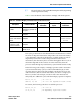
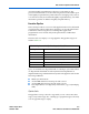
Table Of Contents
- Nios II Processor Reference Handbook
- Contents
- Chapter Revision Dates
- About This Handbook
- Section I. Nios II Processor
- 1. Introduction
- 2. Processor Architecture
- 3. Programming Model
- Introduction
- General- Purpose Registers
- Control Registers
- Operating Modes
- Exception Processing
- Memory and Peripheral Access
- Instruction Set Categories
- Referenced Documents
- Document Revision History
- 4. Instantiating the Nios II Processor in SOPC Builder
- Section II. Appendices
- 5. Nios II Core Implementation Details
- Introduction
- Device Family Support
- Nios II/f Core
- Nios II/s Core
- Nios II/e Core
- Referenced Documents
- Document Revision History
- 6. Nios II Processor Revision History
- 7. Application Binary Interface
- 8. Instruction Set Reference
- Introduction
- Word Formats
- Instruction Opcodes
- Assembler Pseudo- instructions
- Assembler Macros
- Instruction Set Reference
- add
- addi
- and
- andhi
- andi
- beq
- bge
- bgeu
- bgt
- bgtu
- ble
- bleu
- blt
- bltu
- bne
- br
- break
- bret
- call
- callr
- cmpeq
- cmpeqi
- cmpge
- cmpgei
- cmpgeu
- cmpgeui
- cmpgt
- cmpgti
- cmpgtu
- cmpgtui
- cmple
- cmplei
- cmpleu
- cmpleui
- cmplt
- cmplti
- cmpltu
- cmpltui
- cmpne
- cmpnei
- custom
- div
- divu
- eret
- flushd
- flushda
- flushi
- flushp
- initd
- initi
- jmp
- jmpi
- ldb / ldbio
- ldbu / ldbuio
- ldh / ldhio
- ldhu / ldhuio
- ldw / ldwio
- mov
- movhi
- movi
- movia
- movui
- mul
- muli
- mulxss
- mulxsu
- mulxuu
- nextpc
- nop
- nor
- or
- orhi
- ori
- rdctl
- ret
- rol
- roli
- ror
- sll
- slli
- sra
- srai
- srl
- srli
- stb / stbio
- sth / sthio
- stw / stwio
- sub
- subi
- sync
- trap
- wrctl
- xor
- xorhi
- xori
- Referenced Documents
- Document Revision History
Altera Corporation 5–7
October 2007 Nios II Processor Reference Handbook
Nios II Core Implementation Details
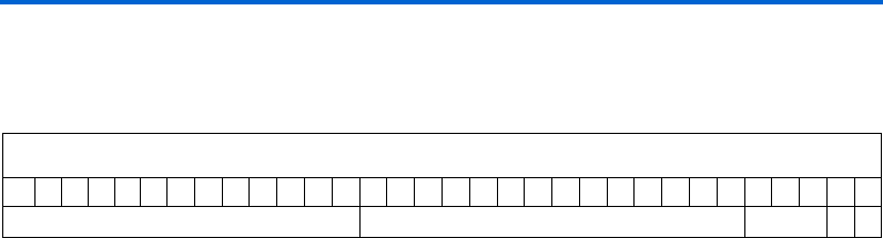
Both the instruction and data cache addresses are divided into fields.
Table 5–4 shows the cache byte address fields.
Instruction Cache
The instruction cache memory has the following characteristics:
■ Direct-mapped cache implementation
■ 32 bytes (8 words) per cache line
■ The instruction master port reads an entire cache line at a time from
memory, and issues one read per clock cycle.
■ Critical word first
The size of the tag field depends on the size of the cache memory and the
physical address size. The size of the line field depends only on the size
of the cache memory. The offset field is always three bits (i.e., an 8-word
line). The maximum instruction byte address size is 31 bits.
The instruction cache is optional. However, excluding instruction cache
from the Nios II/f core requires that the core include at least one tightly-
coupled instruction memory.
Data Cache
The data cache memory has the following characteristics:
■ Direct-mapped cache implementation
■ Configurable line size of 4, 16, or 32 bytes
■ The data master port reads an entire cache line at a time from
memory, and issues one read per clock cycle.
■ Write-back
■ Write-allocate (i.e., store instructions that miss allocate the line for
that address)
The size of the tag field depends on the size of the cache memory and the
physical address size. The size of the line field depends only on the size
of the cache memory. The size of the offset field depends on the line size.
Line sizes of 4, 16, and 32 bytes have offset widths of 0, 2, and 3 bits
respectively. The maximum data byte address size is 31 bits.
The data cache is optional. If the data cache is excluded from the core, the
data master port can also be excluded.
Table 5–4. Cache Byte Address Fields
31... ...210
tag line offset 0 0