Altera Transceiver PHY IP Core User Guide Altera Transceiver PHY IP Core User Guide 101 Innovation Drive San Jose, CA 95134 www.altera.com UG-01080-1.6 Document last updated for Altera Complete Design Suite version: Document publication date: 11.
© 2012 Altera Corporation. All rights reserved. ALTERA, ARRIA, CYCLONE, HARDCOPY, MAX, MEGACORE, NIOS, QUARTUS and STRATIX words and logos are trademarks of Altera Corporation and registered in the U.S. Patent and Trademark Office and in other countries. All other words and logos identified as trademarks or service marks are the property of their respective holders as described at www.altera.com/common/legal.html.
Contents Chapter 1. Introduction PCS . . . . . . . . . . . . . . . . . . . . . . . . . . . . . . . . . . . . . . . . . . . . . . . . . . . . . . . . . . . . . . . . . . . . . . . . . . . . . . . . . . . . 1–2 PMA . . . . . . . . . . . . . . . . . . . . . . . . . . . . . . . . . . . . . . . . . . . . . . . . . . . . . . . . . . . . . . . . . . . . . . . . . . . . . . . . . . . 1–3 Reset Controller . . . . . . . . . . . . . . . . . . . . . . . . . . . . . . . . . . . . . . . . . . . . . . . . . . . . . . . .
iv Contents Stratix V Devices . . . . . . . . . . . . . . . . . . . . . . . . . . . . . . . . . . . . . . . . . . . . . . . . . . . . . . . . . . . . . . . . . . . 4–5 Advanced Options . . . . . . . . . . . . . . . . . . . . . . . . . . . . . . . . . . . . . . . . . . . . . . . . . . . . . . . . . . . . . . . . . . . . 4–9 Configurations . . . . . . . . . . . . . . . . . . . . . . . . . . . . . . . . . . . . . . . . . . . . . . . . . . . . . . . . . . . . . . . . . . . . . . . . . 4–10 Interfaces . . . .
Contents v Register Descriptions . . . . . . . . . . . . . . . . . . . . . . . . . . . . . . . . . . . . . . . . . . . . . . . . . . . . . . . . . . . . . . 6–14 Dynamic Reconfiguration . . . . . . . . . . . . . . . . . . . . . . . . . . . . . . . . . . . . . . . . . . . . . . . . . . . . . . . . . . . . . 6–17 Simulation Files and Example Testbench . . . . . . . . . . . . . . . . . . . . . . . . . . . . . . . . . . . . . . . . . . . . . . . . . . 6–18 Chapter 7.
Contents vi Delay Numbers . . . . . . . . . . . . . . . . . . . . . . . . . . . . . . . . . . . . . . . . . . . . . . . . . . . . . . . . . . . . . . . . . . . . 9–4 Device Family Support . . . . . . . . . . . . . . . . . . . . . . . . . . . . . . . . . . . . . . . . . . . . . . . . . . . . . . . . . . . . . . . . . . . 9–5 Parameter Settings . . . . . . . . . . . . . . . . . . . . . . . . . . . . . . . . . . . . . . . . . . . . . . . . . . . . . . . . . . . . . . . . . . . . . . . 9–6 General Options . .
Contents vii Direct Write Reconfiguration . . . . . . . . . . . . . . . . . . . . . . . . . . . . . . . . . . . . . . . . . . . . . . . . . . . . . . . 10–29 Understanding Logical Channel Numbering . . . . . . . . . . . . . . . . . . . . . . . . . . . . . . . . . . . . . . . . . . . . . . 10–31 Two PHY IP Core Instances Each with Four Bonded Channels . . . . . . . . . . . . . . . . . . . . . . . . . . . . 10–34 One PHY IP Core Instance with Eight Bonded Channels . . . . . . . . . . . . . . . . . . . . . .
viii Altera Transceiver PHY IP Core User Guide Contents March 2012 Altera Corporation
1.
1–2 Chapter 1: Introduction PCS Figure 1–1 illustrates the top level modules that comprise the transceiver PHY IP cores. In addition, Figure 1–1 shows the Altera Transceiver Reconfiguration Controller IP core that is instantiated separately in Stratix V devices. Figure 1–1.
Chapter 1: Introduction PMA 1–3 PMA The PMA receives and transmits differential serial data on the device external pins. The transmit (TX) channel supports programmable pre-emphasis and programmable output differential voltage (VOD). It converts parallel input data streams to serial data. The receive (RX) channel supports offset cancellation to correct for process variation and programmable equalization. It converts serial data to parallel data for processing in the PCS.
1–4 Chapter 1: Introduction Running a Simulation Testbench Running a Simulation Testbench When you generate your transceiver PHY IP core, the Quartus II software generates the HDL files that define your parameterized IP core. In addition, the Quartus II software generates an example Tcl script to compile and simulate your design in ModelSim. Figure 1–2 illustrates the directory structure for the generated files. Figure 1–2. Directory Structure for Generated Files .v or .
Chapter 1: Introduction Unsupported Features 1–5 Table 1–2. Generated Files (Part 2 of 2) File Name Description /_sim/cadence Simulation file for Cadence simulation tools. /_sim/mentor Simulation file for Mentor simulation tools. /_sim/synopsys Simulation file for Synopsys simulation tools.
1–6 Altera Transceiver PHY IP Core User Guide Chapter 1: Introduction Unsupported Features March 2012 Altera Corporation
2. Getting Started This chapter provides a general overview of the Altera IP core design flow to help you quickly get started with any Altera IP core. The Altera IP Library is installed as part of the Quartus II installation process. You can select and parameterize any Altera IP core from the library. Altera provides an integrated parameter editor that allows you to customize IP cores to support a wide variety of applications.
2–2 Chapter 2: Getting Started MegaWizard Plug-In Manager Flow ■ MegaWizard™ Plug-In Manager Flow Figure 2–2.
Chapter 2: Getting Started MegaWizard Plug-In Manager Flow 2–3 2. In the Quartus II software, launch the MegaWizard Plug-in Manager from the Tools menu, and follow the prompts in the MegaWizard Plug-In Manager interface to create or edit a custom IP core variation. 3. To select a specific Altera IP core, click the IP core in the Installed Plug-Ins list in the MegaWizard Plug-In Manager. 4. Specify the parameters on the Parameter Settings pages.
2–4 Chapter 2: Getting Started MegaWizard Plug-In Manager Flow 1 The Finish button may be unavailable until all parameterization errors listed in the messages window are corrected. 8. Click Yes if you are prompted to add the Quartus II IP File (.qip) to the current Quartus II project. You can also turn on Automatically add Quartus II IP Files to all projects. You can now integrate your custom IP core instance in your design, simulate, and compile.
3. 10GBASE-R PHY IP Core The Altera 10GBASE-R PHY IP core implements the functionality described in IEEE 802.3 Clause 49. It delivers serialized data to an optical module that drives optical fiber at a line rate of 10.3125 Gbps. In a multi-channel implementation of 10GBASE-R, each channel of the 10GBASE-R PHY IP core operates independently. Figure 3–1 shows the 10GBASE-R PHY IP core available for Stratix V devices.
3–2 Chapter 3: 10GBASE-R PHY IP Core Release Information To make most effective use of this soft PCS and PMA configuration for Stratix IV GT devices, you can group up to four channels in a single quad and control their functionality using one Avalon-MM PHY management bridge, transceiver reconfiguration module, and low latency controller.
Chapter 3: 10GBASE-R PHY IP Core Device Family Support 3–3 Table 3–1. 10GBASE-R Release Information (Part 2 of 2) Item Description Vendor ID 6AF7 Note to Table 3–1: (1) No ordering codes or license files are required for Stratix V devices. Device Family Support IP cores provide either final or preliminary support for target Altera device families. These terms have the following definitions: ■ Final support—Verified with final timing models for this device.
3–4 Chapter 3: 10GBASE-R PHY IP Core Parameter Settings Stratix V Devices For Stratix V devices, the PCS and PMA are both implemented in hard logic; the 10GBASE-R transceiver PHY requires less than 1% of FPGA resources. Table 3–4 lists the total latency for an Ethernet packet with a 9600 byte payload and an inter-packet gap of 12 characters.
Chapter 3: 10GBASE-R PHY IP Core Parameter Settings 3–5 Table 3–5. General Options (Part 2 of 2) Name Value CMU ATX PLL type Reference Clock Frequency 322.265625 MHz 644.53125 MHz Description You can select either the CMU or ATX PLL. The CMU PLL has a larger frequency range than the ATX PLL. The ATX PLL is designed to improve jitter performance and achieves lower channel-to-channel skew; however, it supports a narrower range of data rates and reference clock frequencies.
3–6 Chapter 3: 10GBASE-R PHY IP Core Parameter Settings Table 3–6. PMA Analog Options (Part 2 of 2) Name Value Description Pre-emphasis pre-tap setting 0–7 Sets the amount of pre-emphasis on the TX buffer. Invert the pre-emphasis pre-tap polarity setting On Off Determines whether or not the pre-emphasis control signal for the pre-tap is inverted. If you turn this option on, the pre-emphasis control signal is inverted.
Chapter 3: 10GBASE-R PHY IP Core Parameter Settings 3–7 Table 3–7 lists the analog parameters for Stratix V devices whose original values are place holders for the values that match your electrical board specification. In Table 3–7, the default value of an analog parameter is shown in bold type. Table 3–7.
3–8 Chapter 3: 10GBASE-R PHY IP Core Parameter Settings Table 3–7. Transceiver and PLL Assignments for Stratix V Devices (Sheet 1 of 2) QSF Assignment Name Pin Planner and Assignment Editor Name VCCA_GXB Voltage XCVR_VCCA_VOLTAGE XCVR_VCCR_VCCT_VOLTAGE VCCR_GXB VCCT_GXB Voltage Description Options Assign To Configure the VCCA_GXB voltage for a GXB I/O pin by specifying the intended VCCA_GXB voltage for a GXB I/O pin.
Chapter 3: 10GBASE-R PHY IP Core Parameter Settings 3–9 Table 3–8. Transceiver and PLL Assignments for Stratix V Devices (Sheet 1 of 3) QSF Assignment Name XCVR_RX_LINEAR_EQUALIZER_ CONTROL Pin Planner and Assignment Editor Name Receiver Linear Equalizer Control Description Options Assign To Static control for the continuous time equalizer in the receiver buffer. The equalizer has 16 distinct settings from 0 –15 corresponding to the increasing AC gain.
3–10 Chapter 3: 10GBASE-R PHY IP Core Parameter Settings Table 3–8.
Chapter 3: 10GBASE-R PHY IP Core Interfaces 3–11 h For more information about the Pin Planner, refer to About the Pin Planner in Quartus II Help. For more information about the Assignment Editor, refer to About the Assignment Editor in Quartus II Help. f For more information about Quartus II Settings, refer to Quartus II Settings File Manual. Interfaces This section describes interfaces of the 10GBASE-R PHY IP Core.
3–12 Chapter 3: 10GBASE-R PHY IP Core Interfaces SDR XGMII TX Interface Table 3–9 describes the signals in the SDR XGMII TX interface. These signals are driven from the MAC to the PCS. This is an Avalon-ST sink interface. Table 3–9. SDR XGMII TX Inputs Signal Name (1) Direction Description Contains 8 lanes of data and control for XGMII. Each lane consists of 8 bits of data and 1 bit of control.
Chapter 3: 10GBASE-R PHY IP Core Interfaces 3–13 Table 3–10.
3–14 Chapter 3: 10GBASE-R PHY IP Core Interfaces Table 3–12 provides the mapping from the XGMII RX interface to the XGMII SDR interface. Table 3–12.
Chapter 3: 10GBASE-R PHY IP Core Interfaces 3–15 The PCS runs at 257.8125 MHz using the pma_rx_clock provided by the PMA. You must provide the PMA a input reference clock running at 644.53725 MHz to generate the 257.8125 MHz clock. Figure 3–4 illustrates the clock generation and distribution for Stratix IV devices. Figure 3–4. Stratix IV GT Clock Generation and Distribution 10GBASE-R Transceiver Channel - Stratix IV GT TX 64 xgmii_tx_clk 40 TX PCS (soft IP) TX PCS (hard IP) 257.8125 MHz 10.
3–16 Chapter 3: 10GBASE-R PHY IP Core Interfaces Figure 3–5 illustrates the clock generation and distribution for Stratix V devices. Figure 3–5. Stratix V Clock Generation and Distribution 10GBASE-R Hard IP Transceiver Channel - Stratix V TX 64 xgmii_tx_clk 10.3125 Gbps serial 40 TX PCS TX PMA 257.8125 MHz RX 64 xgmii_rx_clk TX PLL 10.3125 Gbps serial 40 RX PCS 156.25 MHz pll_ref_clk 644.53125 MHz RX PMA 257.
Chapter 3: 10GBASE-R PHY IP Core Interfaces 3–17 Serial Interface Table 3–15 describes the input and outputs of the transceiver. Table 3–15. Transceiver Serial Interface Signal Name (1) Direction rx_serial_data tx_serial_data Description Input Differential high speed serial input data using the PCML I/O standard. The clock is recovered from the serial data stream. Output Differential high speed serial input data using the PCML I/O standard. The clock is embedded from the serial data stream.
3–18 Chapter 3: 10GBASE-R PHY IP Core Interfaces Register Descriptions Table 3–17 specifies the registers that you can access over the Avalon-MM PHY management interface using word addresses and a 32-bit embedded processor. A single address space provides access to all registers. 1 Writing to reserved or undefined register addresses may have undefined side effects. Table 3–17.
Chapter 3: 10GBASE-R PHY IP Core Interfaces 3–19 Table 3–17. 10GBASE-R Register Descriptions (Part 2 of 3) Word Addr Bit R/W Name Description [31:0] RW reset_fine_control You can use the reset_fine_control register to create your own reset sequence. The reset control module, illustrated in Figure 1–1 on page 1–2, performs a standard reset sequence at power on and whenever the phy_mgmt_clk_reset is asserted. Bits [31:4,0] are reserved.
3–20 Chapter 3: 10GBASE-R PHY IP Core Interfaces Table 3–17. 10GBASE-R Register Descriptions (Part 3 of 3) Word Addr Bit [0] [1] R/W R Name Description For Stratix IV devices, when asserted indicates that the PCS link is up. This bit is only available for Stratix IV devices. PCS_STATUS R When asserted by the BER monitor block, indicates that the PCS is recording a high BER. This bit is only for Stratix IV devices.
Chapter 3: 10GBASE-R PHY IP Core Interfaces 3–21 Table 3–18. External PMA and Reconfiguration Signals (Part 2 of 2) Signal Name Direction cal_blk_pdn Input When asserted, powers down the calibration block. Active high. Input Calibration clock. For Stratix IV devices only. It must be in the range 37.5–50 MHz. You can use the same clock for the phy_mgmt_clk and the cal_blk_clk. Output This is the RX clock, which is recovered from the received data stream.
3–22 Chapter 3: 10GBASE-R PHY IP Core TimeQuest Timing Constraints Although you must initially create a separate reconfiguration interface for each channel and TX PLL in your design, when the Quartus II software compiles your design, it reduces the number of reconfiguration interfaces by merging reconfiguration interfaces. The synthesized design typically includes a reconfiguration interface for three channels.
Chapter 3: 10GBASE-R PHY IP Core TimeQuest Timing Constraints 3–23 Synopsys Design Constraints for Clocks (Continued) #************************************************************** # Create Generated Clocks #************************************************************** create_generated_clock -name pll_mac_clk -source [get_pins -compatibility_mode {*altpll_component|auto_generated|pll1|clk[0]}] create_generated_clock -name pma_tx_clk -source [get_pins -compatibility_mode {*siv_alt_pma|pma_direct|auto_gen
3–24 Chapter 3: 10GBASE-R PHY IP Core Simulation Files and Example Testbench Synopsys Design Constraints for Clocks (Continued) set_false_path -from {*siv_10gbaser_xcvr*clk_reset_ctrl|tx_pma_rstn} -to [get_clocks {{*siv_alt_pma|pma_ch*.pma_direct|receive_pcs*|clkout} {*siv_alt_pma|pma_ch*.
4. XAUI PHY IP Core The Altera XAUI PHY IP core implements the IEEE 802.3 Clause 48 specification to extend the operational distance of the XGMII interface and reduce the number of interface signals. XAUI extends the physical separation possible between the 10 Gbps Ethernet MAC function implemented in an Altera FPGA and the Ethernet standard PHY component on a PCB to one meter. The XAUI IP core accepts 72-bit data (single data rate–SDR XGMII) from the application layer at either 156.25 Mbps or 312.5 Mbps.
4–2 Chapter 4: XAUI PHY IP Core Release Information Release Information Table 4–1 provides information about this release of the XAUI PHY IP core. Table 4–1. XAUI Release Information Item Description Version 11.
Chapter 4: XAUI PHY IP Core Performance and Resource Utilization 4–3 Performance and Resource Utilization Table 4–3 shows the typical expected device resource utilization for different configurations using the current version of the Quartus II software targeting a Stratix IV GX (EP4SG230KF40C2ES) device. Table 4–3. XAUI PHY Performance and Resource Utilization—Stratix IV GX Device Number of 3.125 Gbps Channels Worst-Case Frequency Combinational ALUTs Dedicated Registers Memory Bits Soft XAUI 4 183.
4–4 Chapter 4: XAUI PHY IP Core Parameter Settings Table 4–4. General Options (Part 2 of 2) Name Base data rate Number of XAUI interfaces Value Description 1 × Lane rate 2 × Lane rate 4 × Lane rate The base data rate is the frequency of the clock input to the PLL. Select a base data rate that minimizes the number of PLLs required to generate all the clock s required for data transmission.
Chapter 4: XAUI PHY IP Core Parameter Settings 4–5 Table 4–5. PMA Analog Options (Part 2 of 2) Name Value Description Sets the equalization DC gain using one of the following settings: Receiver DC gain 0–4 Receiver static equalizer setting: 0–15 ■ 0–0 dB ■ 1–3 dB ■ 2–6 dB ■ 3–9 dB ■ 4–12 dB This option sets the equalizer control settings. The equalizer uses a pass band filter. Specifying a low value passes low frequencies. Specifying a high value passes high frequencies.
4–6 Chapter 4: XAUI PHY IP Core Parameter Settings Table 4–6. Transceiver and PLL Assignments for Stratix V Devices (Sheet 1 of 2) QSF Assignment Name XCVR_RX_BYPASS_EQ_ STAGES_234 XCVR_TX_SLEW_RATE_CTRL XCVR_VCCA_VOLTAGE XCVR_VCCR_VCCT_VOLTAGE Altera Transceiver PHY IP Core User Guide Pin Planner and Assignment Editor Name Description Receiver Equalizer Stage 2, 3, 4 Bypass Bypass continuous time equalizer stages 2, 3, and 4 to save power.
Chapter 4: XAUI PHY IP Core Parameter Settings 4–7 Table 4–7 lists the analog parameters with global or computed default values. You may want to optimize some of these settings. In Table 4–7, the default value is shown in bold type. For computed analog parameters, the default value listed is for the initial setting, not the recomputed setting. Table 4–7.
4–8 Chapter 4: XAUI PHY IP Core Parameter Settings Table 4–7. Transceiver and PLL Assignments for Stratix V Devices (Sheet 1 of 3) QSF Assignment Name Pin Planner and Assignment Editor Name Description Options Assign To XCVR_RX_EQ_BW_SEL Receiver Equalizer Gain Bandwidth Select Sets the gain peaking frequency for the equalizer. For data-rates of less than 6.5Gbps set to HALF. For higher datarates set to FULL.
Chapter 4: XAUI PHY IP Core Parameter Settings 4–9 Table 4–7. Transceiver and PLL Assignments for Stratix V Devices (Sheet 1 of 3) Pin Planner and Assignment Editor Name QSF Assignment Name XCVR_TX_VOD XCVR_TX_VOD_PRE_EMP_ CTRL_SRC Description Options Assign To Transmitter Differential Output Voltage Differential output voltage setting. The values are monotonically increasing with the driver main tap current strength.
4–10 Chapter 4: XAUI PHY IP Core Configurations Configurations Figure 4–2 illustrates one configuration of the XAUI IP core. As this figure illustrates, if your variant includes a single instantiation of the XAUI IP core, the transceiver reconfiguration control logic is included in the XAUI PHY IP core. For Stratix V devices the Transceiver Reconfiguration Controller must always be external. Refer to Chapter 10, Transceiver Reconfiguration Controller for more information about this IP core. Figure 4–2.
Chapter 4: XAUI PHY IP Core Interfaces 4–11 Ports Figure 4–3 illustrates the top-level signals of the XAUI PHY IP core for the hard IP implementation. Figure 4–4 illustrates the top-level signals of the XAUI PHY IP core for the soft IP implementation. With the exception of the optional signals available for debugging and the signals for dynamic reconfiguration of the transceivers, the pinout of the two implementations is nearly identical.
4–12 Chapter 4: XAUI PHY IP Core Interfaces Figure 4–4 illustrates the top-level signals of the XAUI PHY IP core for the soft IP implementation for both the single and DDR rates. Figure 4–4.
Chapter 4: XAUI PHY IP Core Interfaces 4–13 For the DDR XAUI variant, the start of control character (0xFB) is aligned to either byte 0 or byte 5. Figure 4–6 illustrates byte 0 alignment. Figure 4–6.
4–14 Chapter 4: XAUI PHY IP Core Interfaces Table 4–9 describes the signals in the SDR TX XGMII interface. Table 4–9. SDR TX XGMII Interface Signal Name Direction Description Contains 4 lanes of data and control for XGMII. Each lane consists of 16 bits of data and 2 bits of control.
Chapter 4: XAUI PHY IP Core Interfaces 4–15 Clocks, Reset, and Powerdown Figure 4–8 illustrates the clock inputs and outputs for the XAUI IP cores with hard PCS and PMA blocks. Figure 4–8. Clock Inputs and Outputs, Hard PCS phy_mgmt_clk XAUI Hard IP Core pll_ref_clk pll_inclk Hard PCS xgmii_tx_clk rx_cruclk PMA 4 tx_coreclk xgmii_rx_clk 4 coreclkout 4 x 3.125 Gbps serial Figure 4–9 illustrates the clock inputs and outputs for the XAUI IP cores with soft PCS and PMA blocks. Figure 4–9.
4–16 Chapter 4: XAUI PHY IP Core Interfaces PMA Channel Controller Table 4–13 describes the signals in this interface. Table 4–13. PMA Channel Controller Signals Signal Name Direction Description cal_blk_powerdown Input Powers down the calibration block. A high-to-low transition on this signal restarts calibration. Only available in Arria II GX and Stratix IV GX, and Stratix IV GT devices. gxb_powerdown Input When asserted, powers down the entire transceiver block.
Chapter 4: XAUI PHY IP Core Interfaces 4–17 Table 4–14. Optional Control and Status Signals Signal Name Direction Description rx_is_lockedtodata[3:0] Output When asserted indicates that the RX CDR PLL is locked to the incoming data. rx_is_lockedtoref[3:0] Output When asserted indicates that the RX CDR PLL is locked to the reference clock. tx_clk312_5 Output This is the clock used for the SDR XGMII interface.
4–18 Chapter 4: XAUI PHY IP Core Interfaces Table 4–15. Optional Control and Status Signals—Hard IP Implementation, Stratix IV GX Devices (Part 2 of 2) Signal Name Direction Description Output Transceiver 8B/10B code group violation or disparity error indicator. If either signal is asserted, a code group violation or disparity error was detected on the associated received code group. Use the rx_disperr signal to determine whether this signal indicates a code group violation or a disparity error.
Chapter 4: XAUI PHY IP Core Interfaces 4–19 Registers The Avalon-MM PHY management interface provides access to the XAUI PHY IP Core PCS, PMA, and transceiver reconfiguration registers. Table 4–16 describes the signals that comprise the Avalon-MM PHY Management interface. Table 4–16. Avalon-MM PHY Management Interface Signal Name Direction Description Avalon-MM clock input.
4–20 Chapter 4: XAUI PHY IP Core Interfaces Table 4–17. XAUI PHY IP Core Registers (Part 2 of 5) Word Addr Bits R/W Register Name Description Reset Control Registers–Automatic Reset Controller 0x041 0x042 [31:0] reset_ch_bitmask Bit mask for reset registers at addresses 0x042 and 0x044. The default value is all 1s. Channel can be reset when bit = 1. W reset_control (write) Writing a 1 to bit 0 initiates a TX digital reset using the reset controller module.
Chapter 4: XAUI PHY IP Core Interfaces 4–21 Table 4–17. XAUI PHY IP Core Registers (Part 3 of 5) Word Addr Bits R/W Register Name Description XAUI PCS [31:4] 0x082 [3:0] — RW Reserved invpolarity[3:0] — Inverts the polarity of corresponding bit on the RX interface. Bit 0 maps to lane 0 and so on. To block: Word aligner. 0x083 [31:4] — Reserved [3:0] RW invpolarity[3:0] — Inverts the polarity of corresponding bit on the TX interface. Bit 0 maps to lane 0 and so on. To block: Serializer.
4–22 Chapter 4: XAUI PHY IP Core Interfaces Table 4–17. XAUI PHY IP Core Registers (Part 4 of 5) Word Addr Bits [31:8] R/W — Description Reserved — Indicates a RX phase compensation FIFO overflow or underrun condition on the corresponding lane. Reading the phase_comp_fifo_error[3: value of the phase_comp_fifo_error register clears the 0] bits. This register is only available in the hard XAUI implementation [7:4] 0x086 Register Name From block: RX phase compensation FIFO.
Chapter 4: XAUI PHY IP Core Interfaces 4–23 Table 4–17. XAUI PHY IP Core Registers (Part 5 of 5) Word Addr 0x089 Bits R/W [31:3] — [2:0] R, sticky Register Name Reserved Description — Indicates a TX phase compensation FIFO overflow or underrun condition on the corresponding lane. Reading the phase_comp_fifo_error[2: value of the phase_comp_fifo_error register clears the bits.This register is only available in the hard XAUI 0] implementation From block: TX phase compensation FIFO.
4–24 Chapter 4: XAUI PHY IP Core Simulation Files and Example Testbench Dynamic Reconfiguration for Stratix V Devices For Stratix V devices, each channel and each TX PLL have separate dynamic reconfiguration interfaces. The parameter editor provides informational messages on the connectivity of these interfaces. Example 4–1 shows the messages for a single transceiver quad.
5. Interlaken PHY IP Core Interlaken is a high speed serial communication protocol for chip-to-chip packet transfers. The Altera Interlaken PHY IP core implements Interlaken Protocol Specification, Rev 1.2. It supports multiple instances, each with 1 to 24 lanes running at up to 10.3125 Gbps on Stratix V devices. The key advantages of Interlaken are scalability and its low I/O count compared to earlier protocols such as SPI 4.2.
5–2 Chapter 5: Interlaken PHY IP Core Device Family Support ■ Lane-based CRC32 ■ Disparity DC balancing f For more detailed information about the Interlaken transceiver channel datapath, clocking, and channel placement, refer to the “Interlaken” section in the Transceiver Protocol Configurations in Stratix V Devices chapter of the Stratix V Device Handbook.
Chapter 5: Interlaken PHY IP Core Parameter Settings 5–3 Table 5–2. General Option (Part 2 of 2) Parameter Value Description Input clock frequency Lane rate/ Lane rate/80 Lane rate/64 Lane rate/50 Lane rate/40 Lane rate/32 Lane rate/25 Lane rate/20 Lane rate/16 Lane rate/12.5 Lane rate/10 Lane rate/8 Specifies the frequency of the input reference clock. The default value for the Input clock frequency is the Lane rate /20; however, you can change this value.
5–4 Chapter 5: Interlaken PHY IP Core Parameter Settings Analog Settings You specify the analog parameters for Stratix V devices using the Quartus II Assignment Editor, the Pin Planner, or through the Quartus II Settings File (.qsf). The default values for analog options fall into three categories: ■ Global— These parameters have default values that are independent of other parameter settings.
Chapter 5: Interlaken PHY IP Core Parameter Settings 5–5 Table 5–4. Transceiver and PLL Assignments for Stratix V Devices (Sheet 1 of 2) QSF Assignment Name Pin Planner and Assignment Editor Name VCCA_GXB Voltage XCVR_VCCA_VOLTAGE XCVR_VCCR_VCCT_VOLTAGE VCCR_GXB VCCT_GXB Voltage Description Options Assign To Configure the VCCA_GXB voltage for a GXB I/O pin by specifying the intended VCCA_GXB voltage for a GXB I/O pin.
5–6 Chapter 5: Interlaken PHY IP Core Parameter Settings Table 5–5. Transceiver and PLL Assignments for Stratix V Devices (Sheet 1 of 3) QSF Assignment Name XCVR_RX_LINEAR_EQUALIZER_ CONTROL Pin Planner and Assignment Editor Name Receiver Linear Equalizer Control Description Options Assign To Static control for the continuous time equalizer in the receiver buffer. The equalizer has 16 distinct settings from 0 –15 corresponding to the increasing AC gain.
Chapter 5: Interlaken PHY IP Core Parameter Settings 5–7 Table 5–5.
5–8 Chapter 5: Interlaken PHY IP Core Interfaces h For more information about the Pin Planner, refer to About the Pin Planner in Quartus II Help. For more information about the Assignment Editor, refer to About the Assignment Editor in Quartus II Help. f For more information about Quartus II Settings, refer to Quartus II Settings File Manual. Interfaces This section describes interfaces of the Interlaken Transceiver PHY.
Chapter 5: Interlaken PHY IP Core Interfaces 5–9 f For more information about _hw.tcl, files refer to the Component Interface Tcl Reference chapter in volume 1 of the Quartus II Handbook. The following sections describe the signals in each interface. Avalon-ST TX Interface Table 5–6 lists the signals in the Avalon-ST TX interface. Table 5–6. Avalon-ST TX Signals Signal Name tx_parallel_data[63:0] Direction Sink Description Avalon-ST data bus driven from the FPGA fabric to the TX PCS.
5–10 Chapter 5: Interlaken PHY IP Core Interfaces Table 5–6. Avalon-ST TX Signals Signal Name Direction Description tx_clkout Output Output clock from the TX PCS. The frequency of this clock equals the Lane rate divided by 40, which is the PMA serialization factor. tx_user_clkout Output Master channel tx_clkout is available when you do not create the optional tx_coreclkin.
Chapter 5: Interlaken PHY IP Core Interfaces 5–11 Table 5–7. Avalon-ST RX Signals (Part 2 of 3) Signal Name Direction Description This is an active-high synchronous status signal indicating that block lock (frame synchronization) and frame lock (metaframe boundary delineation) have been achieved. The Interlaken MAC should use this signal to indicate that Metaframe synchronization has been achieved for this lane.
5–12 Chapter 5: Interlaken PHY IP Core Interfaces Table 5–7. Avalon-ST RX Signals (Part 3 of 3) Signal Name rx_clkout rx_fifo_clr rx_dataout_bp Direction Description Output Output clock from the RX PCS. The frequency of this clock equals the Lane rate divided by 40, which is the PMA serialization factor. Input When asserted, the RX FIFO is flushed. This signal allows you to clear the FIFO if synchronization is not achieved. Sink When asserted, enables reading of data from the RX FIFO.
Chapter 5: Interlaken PHY IP Core Interfaces 5–13 Registers The Avalon-MM PHY management interface provides access to the Interlaken PCS and PMA registers, resets, error handling, and serial loopback controls. You can use an embedded controller acting as an Avalon-MM master to send read and write commands to this Avalon-MM slave interface. Table 5–11 describes the signals that comprise the Avalon-MM management interface. Table 5–11.
5–14 Chapter 5: Interlaken PHY IP Core Interfaces Table 5–12. Interlaken PHY Registers (Part 2 of 3) Word Addr Bits R/W WO 0x042 Register Name reset_control (write) Writing a 1 to bit 0 initiates a TX digital reset using the reset controller module. The reset affects channels enabled in the reset_ch_bitmask. Writing a 1 to bit 1 initiates a RX digital reset of channels enabled in the reset_ch_bitmask. reset_status(read) Reading bit 0 returns the status of the reset controller TX ready bit.
Chapter 5: Interlaken PHY IP Core Interfaces 5–15 Table 5–12. Interlaken PHY Registers (Part 3 of 3) Word Addr Bits R/W Register Name Description Stratix V Device Registers [27] 0x081 [25] R R rx_crc32_err rx_sync_lock Asserted by the CRC32 checker to indicate a CRC error in the corresponding RX lane. From block: CRC32 checker. Asserted by the frame synchronizer to indicate that 4 frame synchronization words have been received so that the RX lane is synchronized.
5–16 Chapter 5: Interlaken PHY IP Core TimeQuest Timing Constraints Table 5–13 describes the signals in the reconfiguration interface. This interface uses the Avalon-MM PHY Management interface clock. Table 5–13. Reconfiguration Interface Signal Name reconfig_to_xcvr [(70)-1:0] reconfig_from_xcvr [(46)-1:0] Direction Description Sink Reconfiguration signals from the Transceiver Reconfiguration Controller. grows linearly with the number of reconfiguration interfaces.
6. PHY IP Core for PCI Express (PIPE) The Altera PHY IP core for PCI Express (PIPE) implements physical coding sublayer (PCS) and physical media attachment (PMA) modules as defined by the Intel PHY Interface for PCI Express (PIPE) Architecture specification. The PHY IP core for PCI Express connects to a PHYMAC for PCI Express to create a complete design. Altera supports the Gen1 and Gen2 specifications and ×1, ×4, or ×8 operation for a total aggregate bandwidth of 2 to 32 Gbps.
6–2 Chapter 6: PHY IP Core for PCI Express (PIPE) Resource Utilization Resource Utilization Table 6–2 shows the typical expected device resource utilization for different configurations using the current version of the Quartus II software targeting a Stratix V GX device. Table 6–2.
Chapter 6: PHY IP Core for PCI Express (PIPE) Parameter Settings 6–3 Table 6–3. General Options (Part 2 of 2) Name PLL type PLL reference clock frequency Value Description CMU ATX You can select either the CMU or ATX PLL. The CMU PLL has a larger frequency range than the ATX PLL. The ATX PLL is designed to improve jitter performance and achieves lower channel-to-channel skew; however, it supports a narrower range of data rates and reference clock frequencies.
6–4 Chapter 6: PHY IP Core for PCI Express (PIPE) Parameter Settings Table 6–4 lists the analog parameters for Stratix V devices whose original values are place holders for the values that match your electrical board specification. In Table 6–4, the default value of an analog parameter is shown in bold type. Table 6–4.
Chapter 6: PHY IP Core for PCI Express (PIPE) Parameter Settings 6–5 Table 6–4. Transceiver and PLL Assignments for Stratix V Devices (Sheet 1 of 2) QSF Assignment Name Pin Planner and Assignment Editor Name VCCA_GXB Voltage XCVR_VCCA_VOLTAGE XCVR_VCCR_VCCT_VOLTAGE VCCR_GXB VCCT_GXB Voltage Description Options Assign To Configure the VCCA_GXB voltage for a GXB I/O pin by specifying the intended VCCA_GXB voltage for a GXB I/O pin.
6–6 Chapter 6: PHY IP Core for PCI Express (PIPE) Parameter Settings Table 6–5. Transceiver and PLL Assignments for Stratix V Devices (Sheet 1 of 3) QSF Assignment Name XCVR_RX_LINEAR_EQUALIZER_ CONTROL Pin Planner and Assignment Editor Name Receiver Linear Equalizer Control Description Options Assign To Static control for the continuous time equalizer in the receiver buffer. The equalizer has 16 distinct settings from 0 –15 corresponding to the increasing AC gain.
Chapter 6: PHY IP Core for PCI Express (PIPE) Parameter Settings 6–7 Table 6–5.
6–8 Chapter 6: PHY IP Core for PCI Express (PIPE) Interfaces h For more information about the Pin Planner, refer to About the Pin Planner in Quartus II Help. For more information about the Assignment Editor, refer to About the Assignment Editor in Quartus II Help. f For more information about Quartus II Settings, refer to Quartus II Settings File Manual. Interfaces This section describes interfaces of the PHY IP Core for PCI Express (PIPE).
Chapter 6: PHY IP Core for PCI Express (PIPE) Interfaces 1 6–9 The block diagram shown in the GUI labels the external pins with the interface type and places the interface name inside the box. The interface type and name are used in the _hw.tcl file. If you turn on Show signals, the block diagram displays all top-level signal names. f For more information about _hw.tcl files, refer to refer to the Component Interface Tcl Reference chapter in volume 1 of the Quartus II Handbook.
6–10 Chapter 6: PHY IP Core for PCI Express (PIPE) Interfaces PIPE Interface Table 6–8 describes the signals in the PIPE interface. Table 6–8. PIPE Interface (Part 1 of 2) Signal Name Direction Description This is the 100 MHz input reference clock source for the PHY PLL. You can optionally provide a 125 MHz input reference clock by setting the PLL reference clock frequency parameter to 125 MHz as described in Table 6–3 on page 6–2.
Chapter 6: PHY IP Core for PCI Express (PIPE) Interfaces 6–11 Table 6–8. PIPE Interface (Part 2 of 2) Signal Name Direction Description This signal requests the PHY to change its power state to the specified state. The following encodings are defined: pipe_powerdown[1:0] (1) Sink ■ 2b’00– P0, normal operation ■ 2b’01–P0s, low recovery time latency, power saving state ■ 2b’10–P1, longer recovery time (64 us maximum latency), lower power state ■ 2b’11–P2, lowest power state.
6–12 Chapter 6: PHY IP Core for PCI Express (PIPE) Interfaces Figure 6–3 illustrates the pipe_pclk switching from Gen1 to Gen2 and back to Gen1. Figure 6–3. Rate Switch from Gen1 to Gen2 250 MHz (Gen1) 500 MHz (Gen2) 250 MHz (Gen1) pipe_pclk pipe_rate T1 T1 pipe_phystatus[-1:0] Note to Figure 6–3: (1) Time T1 is pending characterization. (2) is the number of lanes. Transceiver Serial Interface Table 6–9 describes the differential serial TX and RX connections to FPGA pins. Table 6–9.
Chapter 6: PHY IP Core for PCI Express (PIPE) Interfaces 6–13 Table 6–10. Status Signals (Part 2 of 2) (1) Signal Name Direction Signal Name rx_syncstatus[/8-1:0] Output Indicates presence or absence of synchronization on the RX interface. Asserted when word aligner identifies the word alignment pattern or synchronization code groups in the received data stream. rx_signaldetect[/81:0] Output When asserted indicates that the lane detects a sender at the other end of the link.
6–14 Chapter 6: PHY IP Core for PCI Express (PIPE) Interfaces Table 6–11 describes the signals that comprise the Avalon-MM PHY Management interface. Table 6–11. Avalon-MM PHY Management Interface Signal Name Direction Description Avalon-MM clock input.
Chapter 6: PHY IP Core for PCI Express (PIPE) Interfaces 6–15 Table 6–12. PCI Express PHY (PIPE) IP Core Registers (Part 2 of 4) Word Addr 0x042 Bits R/W Register Name Description W reset_control (write) Writing a 1 to bit 0 initiates a TX digital reset using the reset controller module. The reset affects channels enabled in the reset_ch_bitmask. Writing a 1 to bit 1 initiates a RX digital reset of channels enabled in the reset_ch_bitmask.
6–16 Chapter 6: PHY IP Core for PCI Express (PIPE) Interfaces Table 6–12. PCI Express PHY (PIPE) IP Core Registers (Part 3 of 4) Word Addr Bits R/W Register Name Description 0x066 [31:0] R pma_rx_is_lockedtodata When asserted, indicates that the RX CDR PLL is locked to the RX data, and that the RX CDR has changed from LTR to LTD mode. Bit corresponds to channel . 00x067 [31:0] R pma_rx_is_lockedtoref When asserted, indicates that the RX CDR PLL is locked to the reference clock.
Chapter 6: PHY IP Core for PCI Express (PIPE) Interfaces 6–17 Table 6–12. PCI Express PHY (PIPE) IP Core Registers (Part 4 of 4) Word Addr Bits R/W [31:4] RW [3] RW Register Name Description Reserved rx_bitslip — When set, the word alignment logic operates in bitslip mode. Every time this register transitions from 0 to 1, the RX data slips a single bit. To block: Word aligner.
6–18 Chapter 6: PHY IP Core for PCI Express (PIPE) Simulation Files and Example Testbench For Stratix V devices, each channel and each TX PLL have separate dynamic reconfiguration interfaces. The parameter editor provides informational messages on the connectivity of these interfaces. Example 6–1 shows the messages for a 8-channel PHY IP core for PCI Express (PIPE).
7. Custom PHY IP Core The Altera Custom PHY IP core is a generic PHY that you can customize for use in Arria V or Stratix V FPGAs. You can connect your application’s MAC-layer logic to the Custom PHY to transmit and receive data at rates of 0.611–6.5536 Gbps for Arria V devices or 0.622–8.5 Gbps for Stratix V devices. You can parameterize the physical coding sublayer (PCS) to include the functions that your application requires.
7–2 Chapter 7: Custom PHY IP Core Device Family Support Figure 7–1 illustrates the top-level signals and modules of the Custom PHY. Figure 7–1.
Chapter 7: Custom PHY IP Core Parameter Settings 7–3 Parameter Settings To configure the Custom PHY IP core in the parameter editor, click Installed Plug-Ins > Interfaces > Transceiver PHY > Custom PHY v11.1. You can use the tabs on the parameter editor to select the options required for the protocol. Presets are available for the 1.25 Gbps Ethernet (1.25GbE) protocol. The following sections describe all of the options on seven tabs of the parameter editor and then list parameters that are set for 1.
7–4 Chapter 7: Custom PHY IP Core Parameter Settings Table 7–3. General Options (Part 2 of 3) Name Value Description The PCS-PMA interface width depends on the FPGA fabric transceiver interface width and whether 8B/10B is enabled.
Chapter 7: Custom PHY IP Core Parameter Settings 7–5 Table 7–3. General Options (Part 3 of 3) Name Avalon data interfaces Value Description On/Off When you turn this option On, the order of symbols is changed. This option is typically required if you are planning to import your Custom PHY IP core into a Qsys system. When On, the automatic reset controller resets your design at power up.
7–6 Chapter 7: Custom PHY IP Core Parameter Settings Word Alignment The word aligner restores word boundaries of received data based on a predefined alignment pattern. This pattern can be 7, 8, 10, 16, 20, or 32 bits long. The word alignment module searches for a programmed pattern to identify the correct boundary for the incoming stream. Table 7–5 lists the settings available on the Word Aligner tab. Table 7–5.
Chapter 7: Custom PHY IP Core Parameter Settings 7–7 Table 7–6 provides more information about the word alignment function. Table 7–6. Word Aligner Options Configuration PMA-PCS Interface Width (bits) 8 Custom single deserializer width Word Alignment Mode Manual alignment Word Alignment Pattern Length (bits) 16 Manual alignment 10 16 Custom double deserializer width 20 Automatic synchronized state machine Word Alignment Behavior User-controlled signal starts alignment process.
7–8 Chapter 7: Custom PHY IP Core Parameter Settings Table 7–7. Rate Match FIFO Options (Part 2 of 2) Name Value Rate match insertion/deletion -ve disparity pattern 0010111100 0101111100 Create optional rate match FIFO status ports On/Off Description Enter a 10-bit skip pattern (bits 10–19) and a 10-bit control pattern (bits 0–9). The skip pattern must have neutral disparity.
Chapter 7: Custom PHY IP Core Parameter Settings 7–9 Table 7–9. Byte Order Options Name Value Description Specifies the pattern that identifies the SOP. Byte ordering pattern 11111011 For 16-bit byte ordering pattern you must include a 2-bit pad so that the pattern entered is in the following format: 00 00 . For example, if the required pattern is 10111100, enter the following pattern: 00101111000010111100 Specifies the pad pattern that is inserted to align the SOP.
7–10 Chapter 7: Custom PHY IP Core Parameter Settings Table 7–10. PLL Reconfigurations Name Value Description Channel Interface Turn this option on to enable PLL and datapath dynamic reconfiguration. When you select this option, the width of tx_parallel_data and rx_parallel_data buses increases in the following way.
Chapter 7: Custom PHY IP Core Parameter Settings 7–11 Table 7–11. Transceiver and PLL Assignments for Stratix V Devices (Sheet 1 of 2) QSF Assignment Name XCVR_RX_BYPASS_EQ_ STAGES_234 XCVR_TX_SLEW_RATE_CTRL XCVR_VCCA_VOLTAGE XCVR_VCCR_VCCT_VOLTAGE March 2012 Altera Corporation Pin Planner and Assignment Editor Name Description Receiver Equalizer Stage 2, 3, 4 Bypass Bypass continuous time equalizer stages 2, 3, and 4 to save power.
7–12 Chapter 7: Custom PHY IP Core Parameter Settings Table 7–12 lists the analog parameters with global or computed default values. You may want to optimize some of these settings. In Table 7–12, the default value is shown in bold type. For computed analog parameters, the default value listed is for the initial setting, not the recomputed setting. Table 7–12.
Chapter 7: Custom PHY IP Core Parameter Settings 7–13 Table 7–12. Transceiver and PLL Assignments for Stratix V Devices (Sheet 1 of 3) QSF Assignment Name Pin Planner and Assignment Editor Name Description Options Assign To XCVR_RX_EQ_BW_SEL Receiver Equalizer Gain Bandwidth Select Sets the gain peaking frequency for the equalizer. For data-rates of less than 6.5Gbps set to HALF. For higher datarates set to FULL.
7–14 Chapter 7: Custom PHY IP Core Parameter Settings Table 7–12. Transceiver and PLL Assignments for Stratix V Devices (Sheet 1 of 3) Pin Planner and Assignment Editor Name QSF Assignment Name XCVR_TX_VOD XCVR_TX_VOD_PRE_EMP_ CTRL_SRC Description Options Assign To Transmitter Differential Output Voltage Differential output voltage setting. The values are monotonically increasing with the driver main tap current strength.
Chapter 7: Custom PHY IP Core Interfaces 7–15 Table 7–13. Presets for the 1.25GbE Protocol Parameter Name 1.
7–16 Chapter 7: Custom PHY IP Core Interfaces ■ —The number of lanes ■ —The width of the FPGA fabric to transceiver interface per lane ■ — The symbol size ■ —The number of PLLs Figure 7–2.
Chapter 7: Custom PHY IP Core Interfaces 7–17 The following sections describe the signals in each interface. Avalon-ST TX Input Data from the MAC Table 7–14 describes the signals in the Avalon-ST input interface. These signals are driven from the MAC to the PCS. This is an Avalon sink interface. f For more information about the Avalon-ST protocol, including timing diagrams, refer to the Avalon Interface Specifications. Table 7–14.
7–18 Chapter 7: Custom PHY IP Core Interfaces Clock Interface Table 7–16 describes optional and required clocks for the Custom PHY. The input reference clock, pll_ref_clk, drives a PLL inside the PHY-layer block, and a PLL output clock, rx_clkout (described in Table 7–15 on page 7–17) is used for all data, command, and status inputs and outputs. Table 7–16. Clock Signals Signal Name Direction Description Reference clock for the PHY PLLs. Frequency range is 50–700 MHz.
Chapter 7: Custom PHY IP Core Interfaces 7–19 Table 7–18. Serial Interface and Status Signals (Part 2 of 2) (1) Signal Name Direction Signal Name rx_syncstatus[(/)-1:0] Output Indicates presence or absence of synchronization on the RX interface. Asserted when word aligner identifies the word alignment pattern or synchronization code groups in the received data stream. This signal is optional.
7–20 Chapter 7: Custom PHY IP Core Interfaces Table 7–19. Avalon-ST RX Interface (Part 2 of 2) Signal Name Direction Description rx_digitalreset[-1:0] Input When asserted, resets the RX PCS. rx_analogreset[-1:0] Input When asserted, resets the RX CDR. Output rx_cal_busy[-1:0] When asserted, indicates that the RX channel is being calibrated. You must hold the channel in reset until calibration completes.
Chapter 7: Custom PHY IP Core Interfaces 7–21 Table 7–20 describes the signals in the PHY Management interface. Table 7–20. Avalon-MM PHY Management Interface Signal Name Direction Description phy_mgmt_clk Input Avalon-MM clock input.
7–22 Chapter 7: Custom PHY IP Core Interfaces Table 7–21. Custom PHY IP Core Registers (Part 2 of 3) Word Addr 0x042 Bits R/W Register Name Description W reset_control (write) Writing a 1 to bit 0 initiates a TX digital reset using the reset controller module. The reset affects channels enabled in the reset_ch_bitmask. Writing a 1 to bit 1 initiates a RX digital reset of channels enabled in the reset_ch_bitmask.
Chapter 7: Custom PHY IP Core Interfaces 7–23 Table 7–21. Custom PHY IP Core Registers (Part 3 of 3) Word Addr Bits R/W 0x066 [31:0] R pma_rx_is_lockedtodata When 1, indicates that the RX CDR PLL is locked to the RX data, and that the RX CDR has changed from LTR to LTD mode. Bit corresponds to channel . 0x067 [31:0] R pma_rx_is_lockedtoref When 1, indicates that the RX CDR PLL is locked to the reference clock. Bit corresponds to channel .
7–24 Chapter 7: Custom PHY IP Core Simulation Files and Example Testbench Dynamic Reconfiguration As silicon progresses towards smaller process nodes, circuit performance is affected more by variations due to process, voltage, and temperature (PVT). These process variations result in analog voltages that can be offset from required ranges. The calibration performed by the dynamic reconfiguration interface compensates for variations due to PVT.
8. Low Latency PHY IP Core The Altera Low Latency PHY IP core receives and transmits differential serial data, recovering the RX clock from the RX input stream. The PMA connects to a simplified PCS whose single function doubles the width of the TX and RX datapaths. Depending on the configuration you choose, the Low Latency PHY IP core instantiates one the following the channels: ■ GX channels using the Standard PCS with a frequency range of 1–8.
8–2 Chapter 8: Low Latency PHY IP Core Performance and Resource Utilization Table 8–1 shows the level of support offered by the PMA IP core for Altera device families. Table 8–1.
Chapter 8: Low Latency PHY IP Core Parameter Settings 8–3 Parameter Settings To configure the Low Latency PHY IP core in the MegaWizard Plug-In Manager, click Installed Plug-Ins > Interfaces > Transceiver PHY > Low Latency PHY v11.1. For more information about using the MegaWizard Plug-In Manager refer to Chapter 2, Getting Started. General Options Table 8–3 lists the settings available on General Options tab. Table 8–3.
8–4 Chapter 8: Low Latency PHY IP Core Parameter Settings Table 8–3. General Options Name Value FPGA fabric transceiver interface width PCS-PMA interface width This option indicates the parallel data fabric transceiver interface 8, 10, 16, 20, 32, width. GT datapath supports a single width of 128 bits. Refer 40, 50, 64, 66, 128 toTable 8–4 for the supported interface widths of the Standard and 10G datapaths.
Chapter 8: Low Latency PHY IP Core Parameter Settings 8–5 Table 8–4.
8–6 Chapter 8: Low Latency PHY IP Core Parameter Settings Table 8–5. Additional Options (Part 2 of 2) Name Value Enable rx_coreclkin (1) On/Off Description When you turn this option on, rx_coreclkin connects to the read clock of the RX phase compensation FIFO and you can clock the parallel RX output data using rx_coreclk.
Chapter 8: Low Latency PHY IP Core Parameter Settings 1 8–7 The PLL reconfiguration options are not available for the GT datapath. Table 8–6. PLL Reconfigurations Name Value Description On/Off You must enable this option if you plan to reconfigure the PLLs in your design. This option is also required to simulate PLL reconfiguration. Number of TX PLLs 1–4 Specifies the number of TX PLLs required for this instance of the Low Latency Transceiver PHY.
8–8 Chapter 8: Low Latency PHY IP Core Parameter Settings Analog Options You specify the analog parameters for Stratix V devices using the Quartus II Assignment Editor, the Pin Planner, or through the Quartus II Settings File (.qsf). The default values for analog options fall into three categories: ■ Global— These parameters have default values that are independent of other parameter settings.
Chapter 8: Low Latency PHY IP Core Parameter Settings 8–9 Table 8–7. Transceiver and PLL Assignments for Stratix V Devices (Sheet 1 of 2) QSF Assignment Name Pin Planner and Assignment Editor Name VCCA_GXB Voltage XCVR_VCCA_VOLTAGE XCVR_VCCR_VCCT_VOLTAGE VCCR_GXB VCCT_GXB Voltage Description Options Assign To Configure the VCCA_GXB voltage for a GXB I/O pin by specifying the intended VCCA_GXB voltage for a GXB I/O pin.
8–10 Chapter 8: Low Latency PHY IP Core Parameter Settings Table 8–8. Transceiver and PLL Assignments for Stratix V Devices (Sheet 1 of 3) QSF Assignment Name XCVR_RX_LINEAR_EQUALIZER_ CONTROL Pin Planner and Assignment Editor Name Receiver Linear Equalizer Control Description Options Assign To Static control for the continuous time equalizer in the receiver buffer. The equalizer has 16 distinct settings from 0 –15 corresponding to the increasing AC gain.
Chapter 8: Low Latency PHY IP Core Parameter Settings 8–11 Table 8–8.
8–12 Chapter 8: Low Latency PHY IP Core Interfaces h For more information about the Pin Planner, refer to About the Pin Planner in Quartus II Help. For more information about the Assignment Editor, refer to About the Assignment Editor in Quartus II Help. f For more information about Quartus II Settings, refer to Quartus II Settings File Manual. Interfaces This section describes interfaces of the Low Latency Transceiver PHY.
Chapter 8: Low Latency PHY IP Core Interfaces 8–13 f For more information about _hw.tcl files refer to refer to the Component Interface Tcl Reference chapter in volume 1 of the Quartus II Handbook. The following sections describe each interface. Avalon-ST TX and RX Data Interface to the FPGA Fabric Table 8–9 describes the signals in the Avalon-ST interface.
8–14 Chapter 8: Low Latency PHY IP Core Interfaces Optional Status Interface Table 8–11 describes the signals that comprise the optional status interface. Table 8–11. Optional Status Interface Signal Name Direction Description Output When asserted, indicates that the RX CDR is locked to incoming data. This signal is optional. If latency is not critical, you can read the value of this signal from the Rx_is_lockedtodata register.
Chapter 8: Low Latency PHY IP Core Interfaces 8–15 Table 8–13. Avalon-ST RX Interface (Part 2 of 2) Signal Name Direction Description Input rx_analogreset[-1:0] When asserted, resets the RX CDR. When asserted, indicates that the RX channel is being calibrated. You must hold the channel in reset until calibration completes.
8–16 Chapter 8: Low Latency PHY IP Core Interfaces Table 8–14. Avalon-MM PHY Management Interface (Part 2 of 2) Signal Name Direction Description phy_mgmt_write Input Write signal. phy_mgmt_read Input Read signal. f For more information about the Avalon-MM and Avalon-ST protocols, including timing diagrams, refer to the Avalon Interface Specifications.
Chapter 8: Low Latency PHY IP Core Simulation Files and Example Testbench 8–17 Table 8–15. Low Latency PHY IP Core Registers (Part 2 of 2) Word Addr Bits R/W Register Name Description 0x066 [31:0] R pma_rx_is_lockedtodata When asserted, indicates that the RX CDR PLL is locked to the RX data, and that the RX CDR has changed from LTR to LTD mode. Bit corresponds to channel .
8–18 Altera Transceiver PHY IP Core User Guide Chapter 8: Low Latency PHY IP Core Simulation Files and Example Testbench March 2012 Altera Corporation
9. Deterministic Latency PHY IP Core The Altera Deterministic Latency PHY IP Core targets protocols that require a datapath with deterministic latency. Deterministic latency enables accurate delay measurements and known timing for the transmit (TX) and receive (RX) datapaths as required in applications such as wireless communication systems, emerging Ethernet standards, and test and measurement equipment.
9–2 Chapter 9: Deterministic Latency PHY IP Core and status registers. This is a standard, memory-mapped protocol that is normally used to read and write registers and memory. The transceiver reconfiguration interface connects to the Altera Transceiver Reconfiguration Controller IP core which can dynamically reconfigure transceiver settings. Finally, the PMA transmits and receives serial data which connects to an optical link.
Chapter 9: Deterministic Latency PHY IP Core 9–3 Achieving Deterministic Latency Figure 9–2 illustrates the TX and RX channels when configured as a wireless basestation communicating to a remote radio head (RRH) using a CPRI or OBSAI interface. Figure 9–2 also provides an overview of the calculations that guarantee deterministic delay. As this figure illustrates, you can use a general-purpose PLL to generate the clock that drives the TX CMU PLL or an external reference clock input pin. Figure 9–2.
9–4 Chapter 9: Deterministic Latency PHY IP Core For RE RX_latency_RE = + ( + ) TX_latency_RE = + + For REC RX_latency_REC = + + < rx_clkout phase shift of tx_clkout> TX_latency_REC = +
Chapter 9: Deterministic Latency PHY IP Core Device Family Support 9–5 Table 9–2. TX PCS Total Latency TX Phase Comp FIFO Serializer 8B/10B Bitslip Total Clock Cycles Double word with byte serializer 1.0 0.5 0.5 0 2.0 Double word without byte serializer 1.0 1.0 2.0 0 3.0 Datapath Attributes Table 9–3 shows the total latency through the RX PCS in parallel clock cycles. The RX compensation FIFO is in register mode. Table 9–3.
9–6 Chapter 9: Deterministic Latency PHY IP Core Parameter Settings Parameter Settings To configure the Deterministic Latency PHY IP core in the parameter editor, click Installed Plug-Ins > Interfaces > Transceiver PHY > Deterministic Latency PHY v11.1. You can use the tabs on the parameter editor to select the options required for the protocol. The following sections describe all of the options on the tabs of the parameter editor.
Chapter 9: Deterministic Latency PHY IP Core Parameter Settings 9–7 Table 9–6. General Options (Part 2 of 2) Name Value 1 × Data rate 2 × Data rate 4 × Data rate 8 × Data rate Base data rate Data rate/20 Data rate/10 Data rate/8 Data rate/5 Data rate/4 Data rate/2.5 Data rate/2 Data rate/1.
9–8 Chapter 9: Deterministic Latency PHY IP Core Parameter Settings Additional Options Table 9–8 lists the settings available on the Additional Options tab. Table 9–8. Additional Options (Part 1 of 2) Name Value Description The word aligner restores word boundaries of received data based on a predefined alignment pattern. The word aligner automatically performs an initial alignment to the specified word pattern after reset deassertion.
Chapter 9: Deterministic Latency PHY IP Core Parameter Settings 9–9 Table 9–8. Additional Options (Part 2 of 2) Name Value Description On/Off TX bitslip is enabled whenever the word aligner is in Manual alignment mode. The TX bitslipper uses the value of bitslipboundarselect[4:0] to compensate for bits slipped on the RX datapath to achieve deterministic latency.
9–10 Chapter 9: Deterministic Latency PHY IP Core Parameter Settings Table 9–9 lists the analog parameters for Stratix V devices whose original values are place holders for the values that match your electrical board specification. In Table 9–9, the default value of an analog parameter is shown in bold type. Table 9–9.
Chapter 9: Deterministic Latency PHY IP Core Parameter Settings 9–11 Table 9–9. Transceiver and PLL Assignments for Stratix V Devices (Sheet 1 of 2) QSF Assignment Name Pin Planner and Assignment Editor Name VCCA_GXB Voltage XCVR_VCCA_VOLTAGE XCVR_VCCR_VCCT_VOLTAGE VCCR_GXB VCCT_GXB Voltage Description Options Assign To Configure the VCCA_GXB voltage for a GXB I/O pin by specifying the intended VCCA_GXB voltage for a GXB I/O pin.
9–12 Chapter 9: Deterministic Latency PHY IP Core Parameter Settings Table 9–10. Transceiver and PLL Assignments for Stratix V Devices (Sheet 1 of 3) QSF Assignment Name XCVR_RX_LINEAR_EQUALIZER_ CONTROL Pin Planner and Assignment Editor Name Receiver Linear Equalizer Control Description Options Assign To Static control for the continuous time equalizer in the receiver buffer. The equalizer has 16 distinct settings from 0 –15 corresponding to the increasing AC gain.
Chapter 9: Deterministic Latency PHY IP Core Parameter Settings 9–13 Table 9–10.
9–14 Chapter 9: Deterministic Latency PHY IP Core Interfaces h For more information about the Pin Planner, refer to About the Pin Planner in Quartus II Help. For more information about the Assignment Editor, refer to About the Assignment Editor in Quartus II Help. f For more information about Quartus II Settings, refer to Quartus II Settings File Manual. Interfaces This section describes interfaces of the Deterministic Latency Transceiver PHY.
Chapter 9: Deterministic Latency PHY IP Core Interfaces ■ 9–15
—The number of PLLs Figure 9–3.
9–16 Chapter 9: Deterministic Latency PHY IP Core Interfaces Avalon-ST TX Input Data from the MAC Table 9–11 describes the signals in the Avalon-ST input interface. These signals are driven from the MAC to the PCS. This is an Avalon sink interface. f For more information about the Avalon-ST protocol, including timing diagrams, refer to the Avalon Interface Specifications. Table 9–11.
Chapter 9: Deterministic Latency PHY IP Core Interfaces 9–17 Transceiver Serial Data Interface Table 9–14 describes the differential serial data interface and the status signals for the transceiver serial data interface. Table 9–14. Serial Interface and Status Signals Signal Name (1) Direction rx_serial_data[-1:0] Input tx_serial_data[-1:0] Output Signal Name Receiver differential serial input data. Transmitter differential serial output data.
9–18 Chapter 9: Deterministic Latency PHY IP Core Interfaces Table 9–15. Serial Interface and Status Signals (Part 2 of 2) (1) Signal Name Direction Signal Name rx_is_lockedtodata[((/)-1:0] Output When asserted, the receiver CDR is in to lock-to-data mode. When deasserted, the receiver CDR lock mode depends on the rx_locktorefclk signal level. This signal is optional.
Chapter 9: Deterministic Latency PHY IP Core Interfaces 9–19 Figure 9–4 illustrates the role of the PHY Management module in the Deterministic Latency PHY. Figure 9–4.
9–20 Chapter 9: Deterministic Latency PHY IP Core Interfaces Table 9–17. Avalon-MM PHY Management Interface (Part 2 of 2) Signal Name Direction Input phy_mgmt_read phy_mgmt_waitrequest Output Description Read signal. When asserted, indicates that the Avalon-MM slave interface is unable to respond to a read or write request. When asserted, control signals to the Avalon-MM slave interface must remain constant.
Chapter 9: Deterministic Latency PHY IP Core Interfaces 9–21 Table 9–18. Deterministic Latency PHY IP Core Registers (Part 2 of 3) Word Addr Bits R/W Register Name Description Reset Controls –Manual Mode 0x044 [31:0] RW reset_fine_control You can use the reset_fine_control register to create your own reset sequence. In manual mode, only the TX reset occurs automatically at power on and when the phy_mgmt_clk_reset is asserted.
9–22 Chapter 9: Deterministic Latency PHY IP Core Interfaces Table 9–18. Deterministic Latency PHY IP Core Registers (Part 3 of 3) Word Addr 0x082 Bits R/W Register Name [31:1] R [0] RW Reserved [31:6] RW pcs8g_tx_control [5:1] RW tx_bitslipboundary_select [0] RW tx_invpolarity [31:1] RW Reserved. pcs8g_tx_status 0x083 Description Reserved. — Reserved. Sets the number of bits that the TX bit slipper needs to slip. To block: Word aligner.
Chapter 9: Deterministic Latency PHY IP Core Channel Placement and Utilization 9–23 Although you must initially create a separate reconfiguration interface for each channel and TX PLL in your design, when the Quartus II software compiles your design, it reduces the number of reconfiguration interfaces by merging reconfiguration interfaces. The synthesized design typically includes a reconfiguration interface for three channels.
9–24 Chapter 9: Deterministic Latency PHY IP Core Simulation Files and Example Testbench Figure 9–5 shows the placement of transceiver banks in Arria V devices and indicates the channels that are not available. Figure 9–5.
10. Transceiver Reconfiguration Controller The Altera Transceiver Reconfiguration Controller dynamically reconfigures the analog, channel, and TX PLL settings in Stratix V GX devices. Because the Stratix V FPGA is a 28-nm device, circuit performance is affected by variations due to process, voltage, and temperature (PVT). Stratix V devices that include transceivers must use the Transceiver Reconfiguration Controller to compensate for these variations.
10–2 Chapter 10: Transceiver Reconfiguration Controller This user guide describes the features of the Transceiver Reconfiguration Controller. It also includes descriptions of the accessible transceiver registers, information about the MIF file format, and examples demonstrating the update procedures.
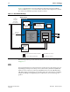
Chapter 10: Transceiver Reconfiguration Controller System Overview 10–3 System Overview Figure 10–1 illustrates the Transceiver Reconfiguration Controller’s role in a Stratix V design. Figure 10–1. Transceiver Reconfiguration Controller Stratix V GX, GS, or GT Device Transceiver PHY Streaming Data TX and RX Serial Data User Application Including MAC Transceiver Reconfiguration Controller Reconfiguration Management Interface S to and from Embedded Controller . . .
10–4 Chapter 10: Transceiver Reconfiguration Controller Device Family Support 1 ■ For more information about Avalon-MM interfaces including timing diagrams, refer to the Avalon Interface Specifications. Streamer Based —This access mode allows you to either stream a MIF that contains the reconfiguration data or perform direct writes to perform reconfiguration. The streaming mode uses a memory initialization file (.mif) to stream an update to the transceiver PHY IP core. The .
Chapter 10: Transceiver Reconfiguration Controller Performance and Resource Utilization 10–5 Performance and Resource Utilization Table 10–3 shows the approximate device resource utilization for a the Transceiver Reconfiguration Controller. The numbers of combinational ALUTs and logic registers are rounded to the nearest 50. Table 10–3 also shows the time required for calibration and AEQ functions. Table 10–3.
10–6 Chapter 10: Transceiver Reconfiguration Controller Parameter Settings Table 10–4 lists the available options. Table 10–4. General Options Name Device family Value Description Arria V Stratix V This IP core is available for Arria V and Stratix V devices. It is not functional for Arria V devices. It is available to establish the correct connections between the transceiver PHY and Transceiver Reconfiguration Controller.
Chapter 10: Transceiver Reconfiguration Controller Interfaces 10–7 Interfaces This section describes interfaces for the Transceiver Reconfiguration Controller. Figure 10–2 illustrates the top-level signals of the Transceiver Reconfiguration Controller. Figure 10–2.
10–8 Chapter 10: Transceiver Reconfiguration Controller Interfaces Transceiver Reconfiguration Interface Table 10–6 describes the signals that comprise the dynamic reconfiguration interface. The Transceiver Reconfiguration Controller communicates with the PHY IP cores using this interface. Table 10–6.
Chapter 10: Transceiver Reconfiguration Controller Reconfiguration Controller Memory Map 10–9 Reconfiguration Controller Memory Map This section describes the memory map that control reconfiguration and signal integrity features. Each register-based feature has its own Avalon-MM address space within the Transceiver Reconfiguration Controller as Figure 10–3 illustrates. Figure 10–3.
10–10 Chapter 10: Transceiver Reconfiguration Controller Transceiver Calibration Functions Table 10–8. Transceiver Reconfiguration Controller Address Map (Part 2 of 2) Address Link 7’h38–7’h3C “Streamer Module” on page 10–22 7’h40–7’h44 “PLL Reconfiguration” on page 10–18 Transceiver Calibration Functions The Transceiver Reconfiguration Controller supports various calibration functions to enhance the performance and operation of any connected transceiver PHY IP core.
Chapter 10: Transceiver Reconfiguration Controller PMA Analog Controls 10–11 PMA Analog Controls You can use the Transceiver Reconfiguration Controller to reconfigure the following analog controls: ■ Differential output voltage (VOD) ■ Pre-emphasis taps ■ Receiver equalization control ■ Receiver equalization DC gain Table 10–9 lists the memory-mapped PMA analog registers that you can access using the reconfiguration management interface. 1 All undefined register bits are reserved. . Table 10–9.
10–12 Chapter 10: Transceiver Reconfiguration Controller EyeQ f Refer to the DC and Switching Characteristics for Stratix V Devices in the Stratix V Device Handbook for the correspondence between the value specified by the reconfiguration data and the actual values that result from these assignments. The actual values are currently pending characterization of Stratix V silicon. 1 All undefined register bits are reserved and must be set to 0. Table 10–10.
Chapter 10: Transceiver Reconfiguration Controller EyeQ 10–13 EyeQ uses a phase interpolator and sampler to estimate the vertical and horizontal eye opening using the values that you specify for the horizontal phase and vertical height. (Refer to Table 10–12 on page 10–14.) The phase interpolator generates a sampling clock and the sampler examines the data from the receiver output. The sampled data is deserialized and sent to the IP core where the PRBS checker determines the BER.
10–14 Chapter 10: Transceiver Reconfiguration Controller DFE Table 10–12 describes the EyeQ registers that you can access. 1 All undefined register bits are reserved and must be set to 0. Table 10–12. EyeQ Offsets and Values Offset 0x0 0x1 0x2 Bits R/W [1] RW [5:0] RW [5:0] RW Register Name Description Control Writing a 1 to this bit enables the Eye monitor.
Chapter 10: Transceiver Reconfiguration Controller DFE 10–15 Table 10–13. DFE Registers (Part 2 of 2) Recon -fig Addr 7’h1A Bits R/W Register Name Description Error. When asserted, indicates an invalid channel or address. [9] R [8] R [1] W Read. Writing a 1 to this bit triggers a read operation. [0] W Write. Writing a 1 to this bit triggers a write operation. control and status Busy. When asserted, indicates that a reconfiguration operation is in progress.
10–16 Chapter 10: Transceiver Reconfiguration Controller AEQ Table 10–14. DFE Offset and Values (Part 2 of 2) Offset Bits R/W Register Name Description Specifies the polarity of the fifth post tap as follows: [3] RW tap 5 polarity 0x5 [2:0] RW tap 5 ■ 0: negative polarity ■ 1: positive polarity Specifies the coefficient for the fifth post tap. The valid range is 0–7.
Chapter 10: Transceiver Reconfiguration Controller ATX PLL Calibration 10–17 Table 10–15. AEQ Registers (Part 2 of 2) Recon -fig Addr 7’h2A Bits R/W Register Name Description Error. When asserted, indicates an error. This bit is asserted when the channel address is invalid. [9] R [8] R [1] W Read. Writing a 1 to this bit triggers a read operation. [0] W Write. Writing a 1 to this bit triggers a write operation. Busy. When asserted, indicates that a reconfiguration operation is in progress.
10–18 Chapter 10: Transceiver Reconfiguration Controller PLL Reconfiguration Table 10–17 lists the direct access ATX registers that you can access using Avalon-MM reads and writes on reconfiguration management interface. 1 All undefined register bits are reserved. Table 10–17. ATX Tuning Registers ATX Addr 7’h30 Bits [9:0] R/W RW [9] Register Name logical channel number R 7’h32 control and status Description The logical channel number.
Chapter 10: Transceiver Reconfiguration Controller PLL Reconfiguration 10–19 You can establish the number of possible PLL configurations on the Reconfiguration tab of the appropriate transceiver PHY IP core. The Reconfiguration tab allows you to specify up to five input reference clocks and up to four TX PLLs. You can also change the input clock source to the CDR PLL; up to five input clock sources are possible.
10–20 Chapter 10: Transceiver Reconfiguration Controller PLL Reconfiguration Table 10–19 lists the PLL reconfiguration registers that you can access using Avalon-MM read and write commands on reconfiguration management interface. 1 All undefined register bits are reserved. Table 10–19. PLL Reconfiguration Registers Addr Bits R/W 7’h40 [9:0] RW 7’h41 [9:0] R Register Name Description logical channel number The logical channel number. Must be specified when performing dynamic updates.
Chapter 10: Transceiver Reconfiguration Controller Channel and PLL Reconfiguration 10–21 Table 10–20 lists the PLL reconfiguration registers. 1 All undefined register bits are reserved and must be set to 0. . Table 10–20. PLL Reconfiguration Offsets and Values Offset Bits R/W Name Description When written initiates reference clock change to the logical reference clock indexed by bits [2:0].
10–22 Chapter 10: Transceiver Reconfiguration Controller Streamer Module ■ Reference clock inputs ■ FPGA fabric transceiver width When you select Enable Channel Interface, in the Custom and Low Latency Transceiver PHY GUIs, the default width of the FPGA fabric to transceiver interface increases for both the Standard and 10G datapaths as follows: ■ Standard datapath—The TX interface is 44 bits. The RX interface is 64 bits. ■ 10G datapath— TX only, RX only, and duplex channels are all 64 bits.
Chapter 10: Transceiver Reconfiguration Controller Streamer Module 1 10–23 All undefined register bits are reserved. Table 10–22. Streamer Module Registers PHY Addr Bits R/W 7’h38 [9:0] RW 7’h39 [9:0] R Register Name Description logical channel number The logical channel number. Must be specified when performing dynamic updates. The Transceiver Reconfiguration Controller maps the logical address to the physical address. physical channel address The physical channel address.
10–24 Chapter 10: Transceiver Reconfiguration Controller Streamer Module Table 10–23 lists the internal Streamer Module registers that you access to control and determine the status of a MIF operation. 1 All undefined register bits are reserved and must be set to 0. Table 10–23. Streamer Module Internal MIF Register Offsets Bits Offset 0x0 0x1 [31:0] R/W RW Register Name MIF base address [2] RW Clear error status [0] RW Start MIF stream Description Specifies the MIF base address.
Chapter 10: Transceiver Reconfiguration Controller Streamer Module 10–25 Mode 1 Avalon-MM Direct Writes for Reconfiguration You specify this mode by writing a value of 2'b01 into bits 2 and 3 of the control and status register, as indicated in Table 10–22 on page 10–23. In this mode, you can write directly to transceiver PHY IP core registers to perform reconfiguration. Refer to “Direct Write Reconfiguration” on page 10–29 for an example of an update using mode 1.
10–26 Chapter 10: Transceiver Reconfiguration Controller Streamer Module For a non-data record, the opcode is represented by the lower 5-bits in the record. Table 10–24 lists the supported opcodes and describes the data content. Table 10–24. Opcodes for MIF Files Opcode Opcode Description 5’b00000 Reserved 5’b00001 Start of MIF Channel format indicator specifying the MIF channel type.
Chapter 10: Transceiver Reconfiguration Controller Procedures for Reconfiguration 10–27 Procedures for Reconfiguration As Table 10–1 indicates, some features can only be reconfigured using register-based accesses, some features can only be reconfigured using MIF-based accesses, and some features can be reconfigured using either access mode. The following sections discuss both modes.
10–28 Chapter 10: Transceiver Reconfiguration Controller Procedures for Reconfiguration 4. Write the control and status register read bit to 1’b1. 5. Read the control and status register busy bit. Continue to read the busy until the value is zero. 6. Read the data register to get the data. Example 10–3 illustrates a read of the pre-emphasis pretap value for logical channel 2. Example 10–3.
Chapter 10: Transceiver Reconfiguration Controller Procedures for Reconfiguration 10–29 Example 10–4 illustrates the reconfiguration of logical channel 0 using a MIF with a base address of 0x100. Example 10–4.
10–30 Chapter 10: Transceiver Reconfiguration Controller Procedures for Reconfiguration In Steps 3 and 4, you must specify an offset value and offset data. You can determine the values of the offset address and offset data by examining the data records specified in either the channel or PLL MIFs. Figure 10–6 shows a sample MIF. Figure 10–6.
Chapter 10: Transceiver Reconfiguration Controller Understanding Logical Channel Numbering 10–31 Example 10–5.
10–32 Chapter 10: Transceiver Reconfiguration Controller Understanding Logical Channel Numbering Figure 10–8 shows the Low Latency PHY IP core GUI specifying 32 channels. The message pane indicates that reconfiguration interfaces 0–31 are for the transceiver channels and reconfiguration interfaces 32–63 are for the TX PLLs. Figure 10–8. Low Latency Transceiver PHY Example 1 After Quartus II compilation, many of the interfaces are merged.
Chapter 10: Transceiver Reconfiguration Controller Understanding Logical Channel Numbering 10–33 Figure 10–9 illustrates the GUI for the Transceiver Reconfiguration Controller. To connect the Low Latency PHY IP core instance to the the Transceiver Reconfiguration Controller, you would enter 64 for Number of reconfiguration interfaces. You would not need to enter any values for the Optional interface grouping parameter because all of the interfaces belong to the same transceiver PHY IP core instance.
10–34 Chapter 10: Transceiver Reconfiguration Controller Understanding Logical Channel Numbering Although you must create a separate logical reconfiguration interface for each PHY IP core instance, when the Quartus II software compiles your design, it reduces original number of logical interfaces by merging them. Allowing the Quartus II software to merge reconfiguration interfaces gives the Fitter more flexibility in placing transceiver channels. However, the logical channel number remains the same.
Chapter 10: Transceiver Reconfiguration Controller Understanding Logical Channel Numbering 10–35 Table 10–25. Channel Ordering for Concatenated Transceiver Instances Logical Interface Number PHY Instance, Interface, or PLL 0–3 Instance 0, interfaces 0–3. 4-7 Instance 0, TX PLL. The Fitter assigns all 4 logical TX PLLs to a single physical PLL. 8-11 Instance 1, interfaces 0–3. 12-15 Instance 1, TX PLL. The Fitter assigns all 4 logical TX PLLs to a single physical PLL.
10–36 Chapter 10: Transceiver Reconfiguration Controller Understanding Logical Channel Numbering 1 Because all of the channels in a transceiver bank share a PLL, this original numbering allows the Fitter to select the optimal CMU PLL from a placement perspective by considering all of the TX PLLs in the bank. Table 10–27 shows the channel numbers for post-Fitter and hardware simulations. At this point, you should have assigned channels to pins of the Stratix V device. Table 10–27.
Chapter 10: Transceiver Reconfiguration Controller Reconfiguration Controller to PHY IP Connectivity 10–37 Reconfiguration Controller to PHY IP Connectivity You can connect a single Transceiver Reconfiguration Controller to all of the transceiver channels and PLLs in your design. You can also use multiple Transceiver Reconfiguration Controllers to facilitate placement and routing of the FPGA.
10–38 Chapter 10: Transceiver Reconfiguration Controller Merging TX PLLs In Multiple Transceiver PHY Instances Merging TX PLLs In Multiple Transceiver PHY Instances The Quartus II Fitter can merge the TX PLLs for multiple transceiver PHY IP cores under the following conditions: ■ The PLLs connect to the same reset pin. ■ The PLLs connect to the same reference clock. ■ The PLLs connect to the same Transceiver Reconfiguration Controller .
Chapter 10: Transceiver Reconfiguration Controller Loopback Modes 10–39 Loopback Modes You can enable the pre- and post-CDR reverse serial loopback modes by writing the appropriate bits of the Transceiver Reconfiguration Controller pma_offset register described in Table 10–9 on page 10–11. In pre-CDR mode, data received through the RX input buffer is looped back to the TX output buffer. In post-CDR mode, received data passes through the RX CDR and then looped back to the TX output buffer.
10–40 Chapter 10: Transceiver Reconfiguration Controller Loopback Modes Figure 10–15 shows the datapath for serial loopback. The data from the FPGA fabric passes through the TX channel and is looped back to the RX channel, bypassing the RX buffer. The received data is available to the FPGA logic for verification. Using the serial loopback option, you can check the operation of all enabled PCS and PMA functional blocks in the TX and RX channels.
11. Migrating from Stratix IV to Stratix V Devices Previously, Altera provided the ALTGX megafunction as a general purpose transceiver PHY solution. The current release of the Quartus II software includes protocol-specific PHY IP cores that simplify the parameterization process. The design of these protocol-specific transceiver PHYs is modular and uses standard interfaces. An Avalon-MM interface provides access to control and status registers that record the status of the PCS and PMA modules.
11–2 Chapter 11: Migrating from Stratix IV to Stratix V Devices Dynamic Reconfiguration of Transceivers This chapter enumerates the differences between the ALTGX megafunction for use with Stratix IV GX devices and the protocol-specific transceiver PHYs for use with Stratix V GX devices in the current release.
Chapter 11: Migrating from Stratix IV to Stratix V Devices XAUI PHY ■ 11–3 reconfig_togxb[3:0]—this single bus connects to all transceiver channels. If you select additional functionality in the parameter editor for the ALTGX_RECONFIG IP core, the IP core adds signals to support that functionality. For more information about the ALTGX_RECONFIG IP core, refer to ALTGX_RECONFIG Megafunction User Guide for Stratix IV Devices in volume 3 of the Stratix IV Device Handbook.
11–4 Chapter 11: Migrating from Stratix IV to Stratix V Devices XAUI PHY Table 11–2. Comparison of ALTGX Megafunction and XAUI PHY Parameters (Part 2 of 2) ALTGX Parameter Name (Default Value) XAUI PHY Parameter Name Comments Acceptable PPM threshold between receiver CDR VCO and receiver input reference clock (±1000) Analog power (Auto) Loopback option (No loopback) Enable static equalizer control (Off) DC gain (0) Receiver common mode voltage (0.
Chapter 11: Migrating from Stratix IV to Stratix V Devices XAUI PHY 11–5 Table 11–3.
11–6 Chapter 11: Migrating from Stratix IV to Stratix V Devices PHY IP Core for PCI Express PHY (PIPE) Table 11–3. Correspondences between XAUI PHY Stratix IV GX and Stratix V Device Signals (Part 3 of 3) (1) Stratix IV GX Devices Signal Name Stratix V Devices Width Signal Name Width 1 phy_mgmt_clk_rst 1 phy_mgmt_clk [8:0] phy_mgmt_address Not available 1 phy_mgmt_read [31:0] phy_mgmt_readdata 1 phy_mgmt_write [31:0] phy_mgmt_writedata Note to Table 11–3: (1) = the number of lanes.
Chapter 11: Migrating from Stratix IV to Stratix V Devices PHY IP Core for PCI Express PHY (PIPE) 11–7 Table 11–4.
11–8 Chapter 11: Migrating from Stratix IV to Stratix V Devices PHY IP Core for PCI Express PHY (PIPE) Table 11–5. PCIe PHY (PIPE) Correspondence between Stratix IV GX Device and Stratix V Device Signals (Part 2 of 3) Stratix IV GX Device Signal Name pll_powerdown cal_blk_powerdown Stratix V Device Signal Name Width These signals are now available as control and status registers.
Chapter 11: Migrating from Stratix IV to Stratix V Devices PHY IP Core for PCI Express PHY (PIPE) 11–9 Table 11–5. PCIe PHY (PIPE) Correspondence between Stratix IV GX Device and Stratix V Device Signals (Part 3 of 3) Stratix IV GX Device Signal Name Stratix V Device Signal Name Width rx_locktodata [-1:0] rx_locktorefclk [-1:0] [-1:0] tx_invpolarity rx_errdetect rx_disperr rx_patterndetect tx_phase_comp_fifo_error (1) These signals are now available as control and status registers.
11–10 Chapter 11: Migrating from Stratix IV to Stratix V Devices Custom PHY Custom PHY This section lists the differences between the parameters and signals for the Custom PHY IP core and the ALTGX megafunction when configured in the Basic functional mode. Parameter Differences Table 11–6 lists the Custom PHY parameters and the corresponding ALTGX megafunction parameters. Table 11–6.
Chapter 11: Migrating from Stratix IV to Stratix V Devices Custom PHY 11–11 Table 11–6.
11–12 Chapter 11: Migrating from Stratix IV to Stratix V Devices Custom PHY Table 11–7. Custom PHY Correspondences between Stratix IV GX Device and Stratix V Device Signals High Speed Serial I/O rx_datain rx_serial_data [-1:0] tx_dataout tx_serial_data [-1:0] rx_freqlocked rx_is_lockedtodata [-1:0] Transceiver Control and Status Signals gxb_powerdown phy_mgmt_clk_reset rx_dataoutfull — tx_dataoutfull — rx_pll_locked There are both pll_locked and rx_pll_clocked in Stratix IV.
Additional Information This chapter provides additional information about the document and Altera. Revision History The table below displays the revision history for the chapters in this user guide. Date Version Changes Made SPR Custom March 2012 1.6 ■ Added register definitions for address range 0x080–0x085. . Low Latency PHY March 2012 1.6 ■ Removed register definitions for address range 0x080–0x085. . 10GBASE-R February 2012 ■ Added datapath latency numbers for Stratix V devices.
Info–2 Additional InformationAdditional Information Revision History Date Version Changes Made SPR Transceiver Reconfiguration Controller February 2012 1.5 ■ Added DFE. Introduction December 2011 1.4 ■ Revised discussion of embedded reset controller to include the fact that this reset controller can be disabled for some transceiver PHYs. 10GBASE-R December 2011 ■ Removed description of calibration block powerdown register (0x021) which is not available for this transceiver PHY.
Additional InformationAdditional Information Revision History Date Info–3 Version Changes Made SPR Transceiver Reconfiguration Controller December 2011 1.4 ■ Added duty cycle distortion (DCD) signal integrity feature. ■ Added PLL and channel reconfiguration using a memory initialization file (.mif).
Info–4 Additional InformationAdditional Information Revision History Date November 2011 Version 1.3 Changes Made SPR ■ Added pll_powerdown bit (bit[0] of 0x044) for manual reset control. You must assert this bit for 1 μs for Gen 2 operation. ■ Added PLL type and base data rate parameters. ■ Updated QSF settings to include text strings used to assign values and location of the assignment which is either a pin or PLL. Custom Transceiver PHY November 2011 1.
Additional InformationAdditional Information Revision History Date Info–5 Version Changes Made SPR All Chapters July 2011 1.2.1 ■ Restricted frequency range of the phy_mgmt_clk to 90–100 MHz for the Transceiver Reconfiguration Controller IP Core chapter.
Info–6 Additional InformationAdditional Information Revision History Date May 2011 Version Changes Made SPR ■ Added support for DDR XAUI ■ Added support for Arria II GZ and HardCopy IV ■ Added example testbench ■ Renamed reconfig_fromgxb and reconfig_togxb reconfig_from_xcvr and reconfig_to_xcvr, respectively. ■ Updated definitions of rx_digital_reset and tx_digital_reset for the soft XAUI implementation in Table 4–17 on page 4–19.
Additional InformationAdditional Information Revision History Date Info–7 Version Changes Made SPR Custom PHY Transceiver May 2011 1.2 ■ Added presets for the 3.25GbE and 1.25GbE protocols. ■ Moved dynamic reconfiguration for the transceiver outside of the Custom PHY IP Core. The reconfiguration signals now connect to a separate Reconfiguration Controller IP Core. ■ Removed device support for Arria II GX, Arria II GZ, HardCopy IV GX, and Stratix IV GX.
Info–8 Additional InformationAdditional Information Revision History Date Version Changes Made SPR All Chapters December 2010 1.11 ■ Corrected frequency range for the phy_mgmt_clk for the Custom PHY IP core in Table 7–20 on page 7–21. ■ Added optional reconfig_from_xcvr[67:0] to Figure 4–4 on page 4–12. Provided more detail on size of reconfig_from_xcvr in Table 4–18 on page 4–23 ■ Removed table providing ordering codes for the Interlaken PHY IP core.
Additional InformationAdditional Information Revision History Date Version Info–9 Changes Made SPR Interlaken PHY Transceiver December 2010 1.1 ■ Added simulation support in ModelSim SE, Synopsys VCS MX, Cadence NCSim ■ Changed number of lanes supported from 4–24 to 1–24. ■ Changed reference clock to be 1/20th rather than 1/10th the lane rate. ■ Renamed management interface, adding phy_ prefix ■ Changed phy_mgmt_address from 16 to 9 bits.
Info–10 Date Additional InformationAdditional Information How to Contact Altera Version November 2010 1.1 July 2010 1.0 Changes Made SPR ■ Corrected address offsets in Table 10–9 on page 10–11. These are byte offsets and should be: 0x00, 0x04, 0x08, 0x0C, 0x10, not 0x00, 0x01, 0x02, 0x03, 0x04. ■ Corrected base address for transceiver reconfiguration control and status registers in Table 10–9 on page 10–11. It should be 0x420, not 0x400.
Additional InformationAdditional Information Typographic Conventions Visual Cue Info–11 Meaning Indicates signal, port, register, bit, block, and primitive names. For example, data1, tdi, and input. The suffix n denotes an active-low signal. For example, resetn. Courier type Indicates command line commands and anything that must be typed exactly as it appears. For example, c:\qdesigns\tutorial\chiptrip.gdf.
Info–12 Altera Transceiver PHY IP Core User Guide Additional InformationAdditional Information Typographic Conventions March 2012 Altera Corporation