
User guide

Chapter 7: Custom PHY IP Core 7–11
Parameter Settings
March 2012 Altera Corporation Altera Transceiver PHY IP Core
User Guide
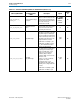
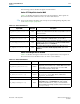
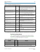
XCVR_RX_BYPASS_EQ_
STAGES_234
Receiver Equalizer Stage 2,
3, 4 Bypass
Bypass continuous time equalizer
stages 2, 3, and 4 to save power. This
setting eliminates significant AC gain
on the equalizer and is appropriate for
chip-to-chip short range
communication on a PCB.
ALL_STAGES_
ENABLED
BYPASS_
STAGES
Pin
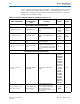
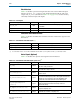
XCVR_TX_SLEW_RATE_CTRL
Transmitter Slew Rate
Control
Specifies the slew rate of the output
signal. The valid values span from the
slowest rate to fastest rate with 1
representing the slowest rate.
1–5
Pin
XCVR_VCCA_VOLTAGE
VCCA_GXB Voltage
Configure the VCCA_GXB voltage for a
GXB I/O pin by specifying the intended
VCCA_GXB voltage for a GXB I/O pin.
If you do not make this assignment the
compiler automatically sets the correct
VCCA_GXB voltage depending on the
configured data rate, as follows:
■ Data rate <= 6.5 Gbps: 2_5V
■ Data rate > 6.5 Gbps: 3_0V or
3_3V for Stratix V ES silicon
2_5V
3_0V
Pin
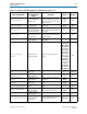
XCVR_VCCR_VCCT_VOLTAGE
VCCR_GXB
VCCT_GXB Voltage
Configure the VCCR_GXB and
VCCT_GXB voltage for an GXB I/O pin
by specifying the intended supply
voltages for a GXB I/O pin. If your
design uses decision feedback
equalization (DFE) or adaptive
equalization (AEQ), you must set this
parameter to 1.0V.
Otherwise, if you do not make this
assignment the compiler
automatically sets the correct
VCCR_GXB and VCCT_GXB voltage
depending on the configured data rate
as follows:
■ Data rate <= 6.5 Gbps: 0_85V
■ Data rate > 6.5 Gbps: 1_0V
0_85V
1_0V
Pin
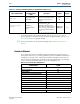
Table 7–11. Transceiver and PLL Assignments for Stratix V Devices (Sheet 1 of 2)
QSF Assignment Name
Pin Planner and
Assignment Editor
Name
Description Options
Assign
To