
User guide

Chapter 8: Low Latency PHY IP Core 8–7
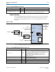
Parameter Settings
March 2012 Altera Corporation Altera Transceiver PHY IP Core
User Guide
1 The PLL reconfiguration options are not available for the GT datapath.
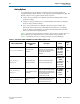
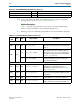
Table 8–6. PLL Reconfigurations
Name Value Description
Allow PLL Reconfiguration On/Off
You must enable this option if you plan to reconfigure the PLLs in
your design. This option is also required to simulate PLL
reconfiguration.
Number of TX PLLs 1–4
Specifies the number of TX PLLs required for this instance of the
Low Latency Transceiver PHY. More than 1 PLL may be required if
your design reconfigures channels to run at multiple frequencies.
Number of input clocks 1–5
Specifies the number of input reference clocks. More than one
reference clock may be required if your design reconfigures channels
to run at multiple frequencies.
Main TX PLL logical index 0–3
Specifies the index for the TX PLL that should be instantiated at
startup. Logical index 0 corresponds to TX PLL0, and so on.
CDR PLL input clock source 0–3
Specifies the index for the TX PLL input clock that should be
instantiated at startup. Logical index 0 corresponds to input clock 0
and so on.
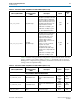
TX PLL (0–3)
(Refer to Table 8–3 on page 8–3 for a detailed explanation of these parameters.)
PLL Type
CMU
ATX
Specifies the PLL type.
Base data rate
1 × Lane rate
2 × Lane rate
4 × Lane rate
Specifies Base data rate.
Input clock frequency Variable
Specifies the frequency of the PLL input reference clock. The
frequency required is the Base data rate/2. You can use any Input
clock frequency that allows the PLLs to generate this frequency.
Select
ed input clock source 0–4
Specifies the index of the input clock for this TX PLL. Logical index 0
corresponds to input clock 0 and so on.
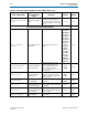
Channel Interface
Enable Channel Interface On/Off
Turn this option on to enable PLL and datapath dynamic
reconfiguration. When you select this option, the width of
tx_parallel_data
and
rx_parallel_data
buses increases in
the following way.
■ Standard datapath:
■ The
tx_parallel_data
bus is 44 bits per lane; however, only
the low-order number of bits specified by the FPGA fabric
transceiver interface width contain valid data for each lane.
■ The
rx_parallel_data
bus is 64 bits per lane; however, only
the low-order number of bits specified by the FPGA fabric
transceiver interface width contain valid data.
■ 10G datapath:
■ The both the
tx_parallel_data
and
rx_parallel_data
buses are 64 bits per lane; however, only the low-order number
of bits specified by the FPGA fabric transceiver interface
width contain valid data.