
User guide

8–14 Chapter 8: Low Latency PHY IP Core
Interfaces
Altera Transceiver PHY IP Core March 2012 Altera Corporation
User Guide
Optional Status Interface
Table 8–11 describes the signals that comprise the optional status interface.
Clock Interface
Table 8–12 describes reference clock for the Low Latency PHY. The input reference
clock,
pll_ref_clk
, drives a PLL inside the PHY-layer block, and a PLL output clock,
rx_clkout
is used for all data, command, and status inputs and outputs.
Reset Control and Status (Optional)
Table 8–13 describes the signals in the optional reset control and status interface.
These signals are available if you do not enable the embedded reset controller. For
more information including timing diagrams, refer to Transceiver Reset Control in
Stratix V Devices in volume 3 of the Stratix V Device Handbook.
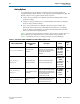
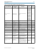
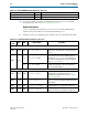
Table 8–11. Optional Status Interface
Signal Name Direction Description
rx_is_lockedtodata[<n>-1:0]
Output
When asserted, indicates that the RX CDR is locked to
incoming data. This signal is optional. If latency is not critical,
you can read the value of this signal from the
Rx_is_lockedtodata
register.
rx_is_lockedtoref[<n>-1:0]
Output
When asserted, indicates that the RX CDR is locked to the input
reference clock. This signal is optional. When the RX CDR is
locked to data, you can ignore transitions on this signal. If
latency is not critical, you can read the value of this signal from
the rx_is_lockedtoref register.
pll_locked[<n>-1:0]
Output
When asserted, indicates that the TX PLL is locked to the input
reference clock. This signal is asynchronous.
tx_bitslip[<n>-1:0]
Output
When set, the data sent to the PMA is slipped. The maximum
number of bits that can be slipped is equal to the value selected
in the serialization factor field - 1 or <d> -1.
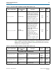
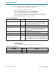
Table 8–12. Clock Signals
Signal Name Direction Description
tx_coreclkin[<n>-1:0]
Input This is an optional clock to drive the write side of the TX FIFO.
rx_coreclkin[<n>-1:0]
Input This is an optional clock to drive the read side of the RX FIFO.
pll_ref_clk
Input
Reference clock for the PHY PLLs. The frequency range is
60–700 MHz.
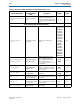
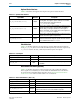
Table 8–13. Avalon-ST RX Interface (Part 1 of 2)
Signal Name Direction Description
pll_powerdown
Input When asserted, resets the TX PLL.
tx_digitalreset[<n>-1:0]
Input When asserted, reset all blocks in the TX PCS.
tx_analogreset[<n>-1:0]
Input When asserted, resets all blocks in the TX PMA.
tx_cal_busy[<n>-1:0]
Output
When asserted, indicates that the TX channel is being calibrated. You
must hold the channel in reset until calibration completes.
rx_digitalreset[<n>-1:0]
Input When asserted, resets the RX PCS.