
User guide


Chapter 8: Low Latency PHY IP Core 8–17
Simulation Files and Example Testbench
March 2012 Altera Corporation Altera Transceiver PHY IP Core
User Guide
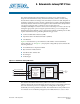
Dynamic Reconfiguration
As silicon progresses towards smaller process nodes, circuit performance is affected
more by variations due to process, voltage, and temperature (PVT). These process
variations result in analog voltages that can be offset from required ranges. The
calibration performed by the dynamic reconfiguration interface compensates for
variations due to PVT.
For Stratix V devices, each channel and each TX PLL have separate dynamic
reconfiguration interfaces.
Although you must initially create a separate reconfiguration interface for each
channel and TX PLL in your design, when the Quartus II software compiles your
design, it reduces the number of reconfiguration interfaces by merging
reconfiguration interfaces. The synthesized design typically includes a
reconfiguration interface for three channels. Allowing the Quartus II software to
merge reconfiguration interfaces gives the Fitter more flexibility in placing transceiver
channels. For more information about transceiver reconfiguration refer to Chapter 10,
Transceiver Reconfiguration Controller.
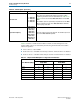
Table 8–16 describes the signals in the reconfiguration interface. This interface uses a
clock provided by the reconfiguration controller.
Simulation Files and Example Testbench
Refer to “Running a Simulation Testbench” on page 1–4 for a description of the
directories and files that the Quartus II software creates automatically when you
generate your Low Latency PHY IP core.
f Refer to the Altera wiki for an example testbench that you can use as a starting point
in creating your own verification environment.
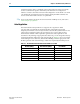
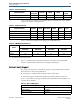
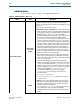
0x066 [31:0] R
pma_rx_is_lockedtodata
When asserted, indicates that the RX CDR PLL is
locked to the RX data, and that the RX CDR has
changed from LTR to LTD mode. Bit <n> corresponds
to channel <n>.
0x067 [31:0] R
pma_rx_is_lockedtoref
When asserted, indicates that the RX CDR PLL is
locked to the reference clock. Bit <n> corresponds to
channel <n>.
Table 8–15. Low Latency PHY IP Core Registers (Part 2 of 2)
Word
Addr
Bits R/W Register Name Description
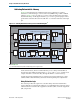
Table 8–16. Reconfiguration Interface
Signal Name Direction Description
reconfig_to_xcvr [(<n>70)-1:0]
Sink
Reconfiguration signals from the Transceiver Reconfiguration
Controller. <n> grows linearly with the number of
reconfiguration interfaces.
reconfig_from_xcvr [(<n>46)-1:0]
Source
Reconfiguration signals to the Transceiver Reconfiguration
Controller. <n> grows linearly with the number of
reconfiguration interfaces.