
User guide

Chapter 9: Deterministic Latency PHY IP Core 9–11
Parameter Settings
March 2012 Altera Corporation Altera Transceiver PHY IP Core
User Guide
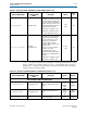
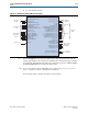
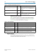
Table 9–10 lists the analog parameters with global or computed default values. You may
want to optimize some of these settings. In Table 9–10, the default value is shown in
bold type. For computed analog parameters, the default value listed is for the initial
setting, not the recomputed setting.
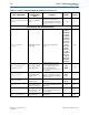
XCVR_VCCA_VOLTAGE
VCCA_GXB Voltage
Configure the VCCA_GXB voltage for a
GXB I/O pin by specifying the intended
VCCA_GXB voltage for a GXB I/O pin.
If you do not make this assignment the
compiler automatically sets the correct
VCCA_GXB voltage depending on the
configured data rate, as follows:
■ Data rate <= 6.5 Gbps: 2_5V
■ Data rate > 6.5 Gbps: 3_0V or
3_3V for Stratix V ES silicon
2_5V
3_0V
Pin
XCVR_VCCR_VCCT_VOLTAGE
VCCR_GXB
VCCT_GXB Voltage
Configure the VCCR_GXB and
VCCT_GXB voltage for an GXB I/O pin
by specifying the intended supply
voltages for a GXB I/O pin. If your
design uses decision feedback
equalization (DFE) or adaptive
equalization (AEQ), you must set this
parameter to 1.0V.
Otherwise, if you do not make this
assignment the compiler
automatically sets the correct
VCCR_GXB and VCCT_GXB voltage
depending on the configured data rate
as follows:
■ Data rate <= 6.5 Gbps: 0_85V
■ Data rate > 6.5 Gbps: 1_0V
0_85V
1_0V
Pin
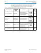
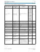
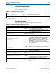
Table 9–9. Transceiver and PLL Assignments for Stratix V Devices (Sheet 1 of 2)
QSF Assignment Name
Pin Planner and
Assignment Editor
Name
Description Options
Assign
To
Table 9–10. Transceiver and PLL Assignments for Stratix V Devices (Sheet 1 of 3)
QSF Assignment Name
Pin Planner and
Assignment Editor
Name
Description Options Assign To
Analog Parameters with Global Default Value
CDR_BANDWIDTH_PRESET
CDR Bandwidth Preset
Specifies the CDR bandwidth preset
setting.
Auto
Low
Medium
High
PLL
instance
PLL_BANDWIDTH_PRESET
PLL Bandwidth Preset
Specifies the PLL bandwidth preset
setting
Auto
Low
Medium
High
PLL
instance
XCVR_RX_DC_GAIN
Receiver Buffer DC Gain
Control
Controls the amount of a stage
receive-buffer DC gain.
0–4 Pin