
User guide

Chapter 9: Deterministic Latency PHY IP Core 9–21
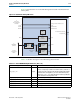
Interfaces
March 2012 Altera Corporation Altera Transceiver PHY IP Core
User Guide
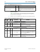
Reset Controls –Manual Mode
0x044
[31:0] RW
reset_fine_control
You can use the
reset_fine_control
register to create
your own reset sequence. In manual mode, only the TX
reset occurs automatically at power on and when the
phy_mgmt_clk_reset
is asserted. When
pma_rx_setlocktodata
or
pma_rx_setlocktodata
is
set, the transceiver PHY is placed in manual mode.
[31:4,0] RW
Reserved
It is safe to write 0s to reserved bits.
[3] RW
reset_rx_digital
Writing a 1 causes the internal RX digital reset signal to be
asserted, resetting the RX digital channels enabled in
reset_ch_bitmask. You must write a 0 to clear the
reset condition.
[2] RW
reset_rx_analog
Writing a 1 causes the internal RX analog reset signal to be
asserted, resetting the RX analog logic of all channels
enabled in reset_ch_bitmask. You must write a 0 to
clear the reset condition.
[1] RW
reset_tx_digital
Writing a 1 causes the internal TX digital reset signal to be
asserted, resetting all channels enabled in
reset_ch_bitmask. You must write a 0 to clear the
reset condition.
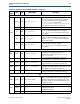
PMA Control and Status Registers
0x061 [31:0] RW
phy
_
serial
_
loopback
Writing a 1 to channel <
n
> puts channel <
n
> in serial
loopback mode. For information about pre- or
post-CDRserial loopback modes, refer to “Loopback
Modes” on page 10–39 .
0x064 [31:0] RW
pma_rx_set_locktodata
When set, programs the RX CDR PLL to lock to the
incoming data. Bit <n> corresponds to channel <n>.
0x065 [31:0] RW
pma_rx_set_locktoref
When set, programs the RX CDR PLL to lock to the
reference clock. Bit <n> corresponds to channel <n>.
0x066 [31:0] R
pma_rx_is_lockedtodata
When asserted, indicates that the RX CDR PLL is locked to
the RX data, and that the RX CDR has changed from LTR to
LTD mode. Bit <n> corresponds to channel <n>.
0x067 [31:0] R
pma_rx_is_lockedtoref
When asserted, indicates that the RX CDR PLL is locked to
the reference clock. Bit <n> corresponds to channel <n>.
PCS
0x080 [31:0] RW Lane or group number
Specifies lane or group number for indirect addressing,
which is used for all PCS control and status registers. For
variants that stripe data across multiple lanes, this is the
logical group number. For non-bonded applications, this is
the logical lane number.
0x081
[31:6] R
pcs8g_rx_status
Reserved.
[5:1] R
rx_bitslipboundaryselect
out
This is an output from the bit slip word aligner which shows
the number of bits slipped.
From block: Word aligner.
[0] R Reserved —
Table 9–18. Deterministic Latency PHY IP Core Registers (Part 2 of 3)
Word
Addr
Bits R/W Register Name Description