
User guide

10–18 Chapter 10: Transceiver Reconfiguration Controller
PLL Reconfiguration
Altera Transceiver PHY IP Core March 2012 Altera Corporation
User Guide
Table 10–17 lists the direct access ATX registers that you can access using Avalon-MM
reads and writes on reconfiguration management interface.
1 All undefined register bits are reserved.
Table 10–18 lists the ATX PLL tuning registers.
Refer to “Changing Transceiver Settings Using Register-Based Reconfiguration” on
page 10–27 for the procedures you can use to control ATX tuning.
PLL Reconfiguration
You can use the PLL reconfiguration registers to change the reference clock input to
the TX PLL or the clock data recovery (CDR) circuitry.
The PLL registers for dynamic reconfiguration feature are available when you select
one of the following Stratix V transceiver PHY IP cores:
■ Custom PHY IP Core
■ Low Latency PHY IP Core
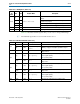
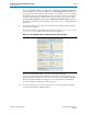
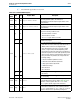
Table 10–17. ATX Tuning Registers
ATX
Addr
Bits R/W Register Name Description
7’h30 [9:0] RW
logical channel number
The logical channel number. The Transceiver Reconfiguration
Controller maps the logical address to the physical address.
7’h32
[9] R
control and status
Error
. When asserted, indicates an invalid channel or
address. This bit is asserted after a write operation if the
selected
logical channel number
selects a logical
channel interface that is not connected to an ATX PLL. It is
also be asserted if the tuning algorithm failed to converge on
a working setting after a manual calibration.
[8] R
Busy
. When asserted, indicates that a reconfiguration
operation is in progress.
[1] W
Read
. Writing a 1 to this bit triggers a read operation.
[0] W
Write
. Writing a 1 to this bit triggers a write operation.
7’h33 [3:0] RW
atx_offset
Specifies the 4-bit register address used for indirect accesses
on the reconfiguration bus. Refer to Table 10–18 for offsets
and values.
7’h34 [15:0] RW
data
Reconfiguration data for the transceiver PHY registers.
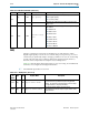
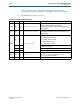
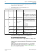
Table 10–18. ATX PLL Tuning Offsets and Values
Offset Bits R/W Register Name Description
0x0 [1] RW
Control
Writing a 1 to this bit triggers ATX PLL
calibration. This register self-clears. Unused bits
of this register must be set to 0.