
User guide

3–10 Chapter 3: 10GBASE-R PHY IP Core
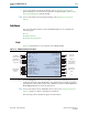
Parameter Settings
Altera Transceiver PHY IP Core March 2012 Altera Corporation
User Guide
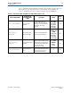
XCVR_TX_COMMON_MODE_
VOLTAGE
Transmitter Common
Mode Driver Voltage
Transmitter common-mode driver
voltage
VOLT_0P80V
VOLT_0P75V
VOLT_0P70V
VOLT_0P65V
VOLT_0P60V
VOLT_0P55V
VOLT_0P50V
VOLT_0P35V
PULL_UP
PULL_DOWN
TRISTATED1
GROUNDED
PULL_UP_TO
VCCELA
TRISTATED2
TRISTATED3
TRISTATED4
Pin
XCVR_TX_PRE_EMP_1ST_POST_
TAP
Transmitter Preemphasis
First Post-Tap
Specifies the first post-tap setting
value.
0 –31
Pin
XCVR_TX_PRE_EMP_2ND_
POST_TAP
Transmitter Preemphasis
Second Post-Tap
Specifies the second post-tap setting
value.
0–15
Pin
XCVR_TX_PRE_EMP_INV_
2ND_TAP
Transmitter Preemphasis
Second Tap Invert
Inverts the transmitter pre-emphasis
2nd post tap.
TRUE
FALSE
Pin
XCVR_TX_PRE_EMP_INV_
PRE_TAP
Transmitter Preemphasis
Pre Tap Invert
Inverts the transmitter pre-emphasis
pre-tap.
TRUE
FALSE
Pin
XCVR_TX_PRE_EMP_PRE_TAP
Transmitter Preemphasis
Pre-Tap
Specifies the pre-tap pre-emphasis
setting.
0 –15
Pin
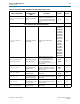
XCVR_TX_RX_DET_ENABLE
Transmitter's Receiver
Detect Block Enable
Enables or disables the receiver
detector circuit at the transmitter.
TRUE
FALSE
Pin
XCVR_TX_RX_DET_MODE
Transmitter's Receiver
Detect Block Mode
Sets the mode for receiver detect block 0–15
Pin
XCVR_TX_RX_DET_OUTPUT_SEL
Transmitter's Receiver
Detect Block QPI/PCI
Express Control
Determines QPI or PCI Express mode
for the Receiver Detect block.
RX_DET_QPI_
OUT
RX_DET_PCIE_
OUT
Pin
XCVR_TX_VOD
Transmitter Differential
Output Voltage
Differential output voltage setting. The
values are monotonically increasing
with the driver main tap current
strength.
0–63
50
Pin
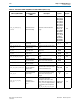
XCVR_TX_VOD_PRE_EMP_
CTRL_SRC
Transmitter V
OD
/
Preemphasis Control
Source
When set to
DYNAMIC_CTL
, the PCS
block controls the V
OD
and
preemphasis coefficients for PCI
Express. When this assignment is set
to
RAM_CTL
the V
OD
and preemphasis
are controlled by other assignments,
such as
XCVR_TX_PRE_EMP_1ST_POST_TAP
.
DYNAMIC_CTL
RAM_CTL
Pin
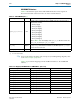
Table 3–8. Transceiver and PLL Assignments for Stratix V Devices (Sheet 1 of 3)
QSF Assignment Name
Pin Planner and
Assignment Editor
Name
Description Options Assign To