
User guide

5–4 Chapter 5: Interlaken PHY IP Core
Parameter Settings
Altera Transceiver PHY IP Core March 2012 Altera Corporation
User Guide
Analog Settings
You specify the analog parameters for Stratix V devices using the Quartus II
Assignment Editor, the Pin Planner, or through the Quartus II Settings File (.qsf). The
default values for analog options fall into three categories:
■ Global— These parameters have default values that are independent of other
parameter settings.
■ Computed—These parameters have an initial default value that is recomputed
based on other parameter settings.
■ Proxy—These parameters have default values that are place holders. The
Quartus II software selects these initial default values based on your design;
however, Altera recommends that you replace these defaults with values that
match your electrical board specification.
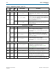
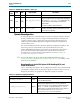
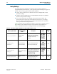
Table 5–4 lists the analog parameters for Stratix V devices whose original values are
place holders for the values that match your electrical board specification. In
Table 5–4, the default value of an analog parameter is shown in bold type.
Table 5–4. Transceiver and PLL Assignments for Stratix V Devices (Sheet 1 of 2)
QSF Assignment Name
Pin Planner and
Assignment Editor
Name
Description Options
Assign
To
XCVR_IO_PIN_TERMINATION
Transceiver I/O Pin
Termination
Specifies the intended on-chip
termination value for the specified
transceiver pin. Use External Resistor
if you intend to use off-chip
termination.
85_OHMS
100_OHMS
120_OHMS
150_OHMS
EXTERNAL_
RESISTOR
Pin
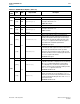
XCVR_REFCLK_PIN_
TERMINATION
Transceiver Dedicated
Refclk Pin Termination
Specifies the intended termination
value for the specified refclk pin.
DC_COUPLING_
INTERNAL_100
_OHM
DC_COUPLING_
EXTERNAL_
RESISTOR
AC_COUPLING
Pin
XCVR_RX_BYPASS_EQ_
STAGES_234
Receiver Equalizer Stage 2,
3, 4 Bypass
Bypass continuous time equalizer
stages 2, 3, and 4 to save power. This
setting eliminates significant AC gain
on the equalizer and is appropriate for
chip-to-chip short range
communication on a PCB.
ALL_STAGES_
ENABLED
BYPASS_
STAGES
Pin
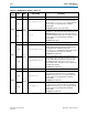
XCVR_TX_SLEW_RATE_CTRL
Transmitter Slew Rate
Control
Specifies the slew rate of the output
signal. The valid values span from the
slowest rate to fastest rate with 1
representing the slowest rate.
1–5
Pin