
User guide

Chapter 7: Functional Description—High-Performance Controller II 7–25
Register Maps Description
December 2010 Altera Corporation External Memory Interface Handbook Volume 3
Section II. DDR3 SDRAM Controller with ALTMEMPHY IP User Guide
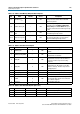
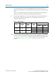
Table 7–20. Address 0x126 Memory Timing Parameters Register 3
Bit Name Default Access Description
3:0 CAS latency, t
CL
—RW
This value must be set to match the memory CAS
latency. You must set this value in the 0x04
register map as well.
7:4 Additive latency, AL — RW
Additive latency setting. The default value for
these bits is set in the Memory additive CAS
latency setting in the Preset Editor dialog box.
You must set this value in the 0x05 register map
as well.
11:8
CAS write latency,
CWL
—RW
CAS write latency setting. You must set this value
in the 0x06 register map as well.
15:12 Write recovery, t
WR
—RW
This value must be set to match the memory
write recovery time (t
WR
). You must set this
value in the 0x04 register map as well.
31:16 Reserved 0 — Reserved for future use.
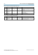
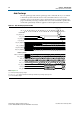
Table 7–21. Address 0x130 ECC Control Register
Bit Name Default Access Description
0 ENABLE_ECC 1 RW
When 1, enables the generation and checking
of ECC.
1 ENABLE_AUTO_CORR — RW
When 1, enables auto-correction when a
single-bit error is detected.
2 GEN_SBE 0 RW
When 1, enables the deliberate insertion of
single-bit errors, bit 0, in the data written to
memory. This bit is only used for testing
purposes.
3 GEN_DBE 0 RW
When 1, enables the deliberate insertion of
double-bit errors, bits 0 and 1, in the data
written to memory. This bit is only used for
testing purposes.
4 ENABLE_INTR 1 RW When 1, enables the interrupt output.
5 MASK_SBE_INTR 0 RW When 1, masks the single-bit error interrupt.
6 MASK_DBE_INTR 0 RW When 1, masks the double-bit error interrupt
7CLEAR 0 RW
When 1, writing to this self-clearing bit clears
the interrupt signal, and the error status and
error address registers.
9 Reserved 0 — Reserved for future use.
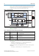
Table 7–22. Address 0x131 ECC Status Register (Part 1 of 2)
Bit Name Default Access Description
0 SBE_ERROR 0 RO Set to 1 when any single-bit errors occur.
1 DBE_ERROR 0 RO Set to 1 when any double-bit errors occur.
7:2 Reserved 0 — Reserved for future use.