
User guide

Chapter 9: Timing Diagrams 9–25
DDR3 High-Performance Controllers II
December 2010 Altera Corporation External Memory Interface Handbook Volume 3
Section II. DDR3 SDRAM Controller with ALTMEMPHY IP User Guide
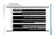
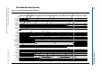
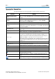
The following sequence corresponds with the numbered items in Figure 9–14:
1. The user logic asserts the first
local_write_req
signal with a size of 1 and an
address of
0×000000
. The
local_ready
signal is asserted along with the
local_write_req
signal, which indicates that the controller has accepted this
request, and the user logic can request another read or write in the following clock
cycle. If the
local_ready
signal was not asserted, the user logic must keep the
write request, size, and address signals asserted until the
local_ready
signal is
registered high. The local address
0x000000
is mapped to the following memory
address in half-rate mode:
mem_row_address = 0×0000
mem_col_address = 0×0000<<2 = 0×0000
mem_bank_address = 0×00
2. The user logic asserts a second
local_write_req
signal with a size of 1 and
address of 1. The
local_ready
signal is asserted along with the
local_write_req
signal, which indicates that the controller has accepted this request. Since the
second write request is to a sequential address (same row, same bank, and column
increment by 1), this write and the first write can be merged at the memory
transaction.
3. The controller issues the necessary memory command and address signals to the
ALTMEMPHY megafunction for it to send to the memory device.
4. The controller asserts the
afi_wdata_valid
signal to indicate to the ALTMEMPHY
megafunction that valid write data and write data masks are present on the inputs
to the ALTMEMPHY megafunction.
5. The controller asserts the
afi_dqs_burst
signals to control the timing of the DQS
signal that the ALTMEMPHY megafunction issues to the memory.
6. The ALTMEMPHY megafunction issues the write command, and sends the write
data and write DQS to the memory.