
User guide

3–6 Chapter 3: Parameter Settings
ALTMEMPHY Parameter Settings
External Memory Interface Handbook Volume 3 December 2010 Altera Corporation
Section II. DDR3 SDRAM Controller with ALTMEMPHY IP User Guide
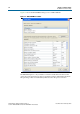
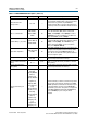
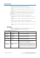
Row address width 12–16 bits
Defines the number of row address bits for your
interface. If your DDR3 SDRAM device’s row address bus
is 12-bit wide, set the row address width to 13 and set the
13
th
bit to logic-level low (or leave the 13
th
bit
unconnected to the memory device) in the top-level file.
Bank address width 3 bits
Defines the number of bank address bits for your
interface.
Chip selects per DIMM 1 or 2 bits
Defines the number of chip selects on each DIMM in your
interface. Currently, calibration is done with all ranks but
you can only perform timing analysis with one
single-rank DIMM.
DQ bits per DQS bit 4 or 8 bits
Defines the number of data (DQ) bits for each data strobe
(DQS) pin.
Drive DM pins from FPGA Yes or No —
Specifies whether you are using DM pins for write
operation. Altera devices do not support DM pins with ×4
mode.
Maximum memory frequency
for CAS latency 5.0
80–700 MHz
Specifies the frequency limits from the memory data
sheet per given CAS latency. The ALTMEMPHY
MegaWizard Plug-In Manager generates a warning if the
operating frequency with your chosen CAS latency
exceeds this number. The lowest frequency supported by
DDR3 SDRAM devices is 300 MHz.
Maximum memory frequency
for CAS latency 6.0
Maximum memory frequency
for CAS latency 7.0
Maximum memory frequency
for CAS latency 8.0
Maximum memory frequency
for CAS latency 9.0
Maximum memory frequency
for CAS latency 10.0
Note to Table 3–3:
(1) The range values depend on the actual memory device used.
Table 3–3. DDR3 SDRAM Attributes Settings (Part 2 of 2)
Parameter Name Range (1) Units Description
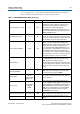
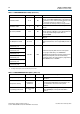
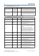
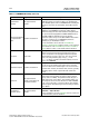
Table 3–4. DDR3 SDRAM Initialization Options (Part 1 of 3)
Parameter Name Range Units Description
Memory burst length 4, 8, on-the-fly beats
Sets the number of words read or written per
transaction.
Memory burst ordering
Sequential or
Interleaved
—
Controls the order in which data is transferred between
memory and the FPGA during a read transaction. For
more information, refer to the memory device
datasheet.
DLL precharge power down
Fast exit or Slow
exit
—
Sets the mode register setting to disable (Slow exit) or
enable (Fast exit) the memory DLL when CKE is
disabled.