
User guide

3–10 Chapter 3: Parameter Settings
ALTMEMPHY Parameter Settings
External Memory Interface Handbook Volume 3 December 2010 Altera Corporation
Section II. DDR3 SDRAM Controller with ALTMEMPHY IP User Guide
Derating Memory Setup and Hold Timing
Because the base setup and hold time specifications from the memory device
datasheet assume input slew rates that may not be true for Altera devices, derate and
update the following memory device specifications in the Preset Editor dialog box:
■ t
DS
■ t
DH
■ t
IH
■ t
IS
1 For Arria II GX and Stratix IV devices, you need not derate using the Preset Editor.
You only need to enter the parameters referenced to V
REF
, and the deration is done
automatically when you enter the slew rate information on the Board Settings tab.
After derating the values, you then need to normalize the derated value because
Altera input and output timing specifications are referenced to V
REF
. When the
memory device setup and hold time numbers are derated and normalized to V
REF
,
update these values in the Preset Editor dialog box to ensure that your timing
constraints are correct.
The following memory device specifications and update the Preset Editor dialog box
with the derated value:
For example, according to JEDEC, 533-MHz DDR3 SDRAM has the following
specifications, assuming 1V/ns DQ slew rate rising signal and 2V/ns DQS-DQSn
slew rate:
■ Base t
DS
= 25
■ Base t
DH
= 100
■ V
IH
(ac) = V
REF
+ 0.175 V
■ V
IH
(dc) = V
REF
+ 0.100 V
■ V
IL
(ac) = V
REF
– 0.175 V
■ V
IL
(dc) = V
REF
– 0.100 V
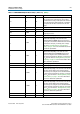
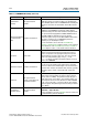
t
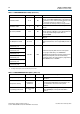
RRD
2.06–64 ns
The activate to activate time, per device, RAS to RAS
delay timing parameter.
t
FAW
7.69–256 ns The four-activate window time, per device.
t
RTP
2.06–64 ns Read to precharge time.
Note to Table 3–5:
(1) See the memory device data sheet for the parameter range. Some of the parameters may be listed in a clock cycle (t
CK
) unit. If the MegaWizard
Plug-In Manager requires you to enter the value in a time unit (ps or ns), convert the number by multiplying it with the clock period of your
interface (and not the maximum clock period listed in the memory data sheet).
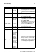
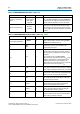
Table 3–5. DDR3 SDRAM Timing Parameter Settings (Part 3 of 3) (Note 1)
Parameter Name Range Units Description