
User guide

3–12 Chapter 3: Parameter Settings
ALTMEMPHY Parameter Settings
External Memory Interface Handbook Volume 3 December 2010 Altera Corporation
Section II. DDR3 SDRAM Controller with ALTMEMPHY IP User Guide
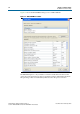
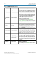
Instantiate DLL
externally
All supported device
families.
Use this option with Stratix III, Stratix IV, HardCopy III, or
HardCopy IV devices, if you want to apply a non-standard phase
shift to the DQS capture clock. The ALTMEMPHY DLL offsetting I/O
can then be connected to the external DLL and the Offset Control
Block.
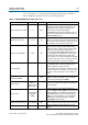
Enable dynamic parallel
on-chip termination
(OCT)
Stratix III and Stratix IV
This option provides I/O impedance matching and termination
capabilities. The ALTMEMPHY megafunction enables parallel
termination during reads and series termination during writes with
this option checked. Only applicable for DDR3 SDRAM interfaces
where DQ and DQS are bidirectional. Using the dynamic
termination requires that you use the OCT calibration block, which
may impose a restriction on your DQS/DQ pin placements
depending on your R
UP
/R
DN
pin locations.
For more information, refer to either the External Memory
Interfaces in Stratix III Devices chapter in volume 1 of the Stratix III
Device Handbook or the External Memory Interfaces in Stratix IV
Devices chapter in volume 1 of the Stratix IV Device Handbook.
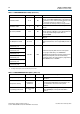
Clock phase Arria II GX
Adjusting the address and command phase can improve the
address and command setup and hold margins at the memory
device to compensate for the propagation delays that vary with
different loadings. You have a choice of 0°, 90°, 180°, and 270°,
based on the rising and falling edge of the
phy_clk
and
write_clk
signals. In Stratix IV and Stratix III devices, the clock
phase is set to dedicated.
Dedicated clock phase Stratix III and Stratix IV
When you use a dedicated PLL output for address and command,
you can choose any legal PLL phase shift to improve setup and
hold for the address and command signals. You can set this value
to between 180° and 359° (the default is 240°). However, generally
PHY timing requires a value of greater than 240° for half-rate
designs.
Board skew
All supported device
families except Arria II GX
and Stratix IV devices
Maximum skew across any two memory interface signals for the
whole interface from the FPGA to the memory (either a discrete
memory device or a DIMM). This parameter includes all types of
signals (data, strobe, clock, address, and command signals). You
need to input the worst-case skew, whether it is within a DQS/DQ
group, or across all groups, or across the address and command
and clocks signals. This parameter generates the timing constraints
in the .sdc file.
Autocalibration
simulation options
All supported device
families
Choose between Full Calibration (long simulation time), Quick
Calibration, or Skip Calibration.
For more information, refer to the Simulation section in volume 4 of
the External Memory Interface Handbook.
Table 3–6. ALTMEMPHY PHY Settings (Part 2 of 2)
Parameter Name Applicable Device Families Description