
User guide


Chapter 5: Functional Description—ALTMEMPHY 5–5
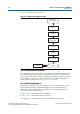
Block Description
December 2010 Altera Corporation External Memory Interface Handbook Volume 3
Section II. DDR3 SDRAM Controller with ALTMEMPHY IP User Guide
■ Mixed:
‘b0011
- DDIO high and low bits have to toggle
Loading a mixed pattern is complex, because write latency is unknown at this time.
Two sets of write and read operations (single pin resynchronization (capture) clock
phase sweeps, (“Step 3: Read Resynchronization (Capture) Clock Phase”) are required
to accurately write the mixed pattern to memory.
1 Memory bank 0, row 0, and column addresses 0 to 55 store calibration data.
Step 3: Read Resynchronization (Capture) Clock Phase
This step adjusts the phase of the resynchronization clock to determine the optimal
phase that gives the greatest margin. The resynchronization clock captures the
outputs of DQS capture registers (DQS is the capture clock).
To correctly calibrate resynchronization clock phase, based on a data valid window,
requires 720° of phase sweep.
Step 4: Read and Write Datapath Timing
In this step, the sequencer calculates the calibrated write latency (the
ctl_wlat
signal)
between write commands and write data. The sequencer also calculates the calibrated
read latency (the
ctl_rlat
signal) between the issue of a read command and valid
read data. Both read and write latencies are output to a controller. In addition to
advertising the read latency, the sequencer calibrates a read data valid signal to the
delay between a controller issuing a read command and read data returning. The
controller can use the read data valid signal in place of the advertised read latency, to
determine when the read data is valid.
Step 5: Address and Command Clock Cycle
This step optionally adds an additional memory clock cycle of delay from the address
and command path. This delay aligns the write data to the memory commands given
in the controller clock domain. If you require this delay, this step reruns the calibration
(“Step 2: Write Training Patterns” to “Step 4: Read and Write Datapath Timing”) to
calibrate to the new setting.
Step 6: Postamble
This step sets the correct clock cycle for the postamble path. The aim of the postamble
path is to eliminate false DQ data capture because of postamble glitches on the DQS
signal, through an override on DQS. This step ensures the correct clock cycle timing of
the postamble enable (override) signal.
Step 7: Prepare for User Mode
In this step, the PHY applies user mode register settings and performs periodic VT
tracking.
VT Tracking
VT tracking is a background process that tracks the voltage and temperature
variations to maintain the relationship between the resynchronization or capture
clock and the data valid window that are achieved at calibration.