
User guide


Chapter 5: Functional Description—ALTMEMPHY 5–11
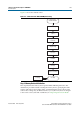
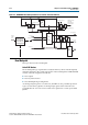
Block Description
December 2010 Altera Corporation External Memory Interface Handbook Volume 3
Section II. DDR3 SDRAM Controller with ALTMEMPHY IP User Guide
Step 7: Write Clock Path Setup
After the sequencer has the optimum settings for read capture and resynchronization
setup, the sequencer calibrates the write datapath by configuring the alignment
registers in the IOE and the DQ and DQS phase shift per DQS group. This step
ensures that the write data can be presented on the same clock cycle from controller,
but launched at the appropriate time for each DQS group to the DDR3 SDRAM
memory devices.
Step 8: Prepare for User Mode
In this step, the sequencer sends the calibrated write latency between command and
write data (the
ctl_wlat
signal) to the controller. The PHY then applies user mode
register settings and performs setup for periodic VT tracking.
1 Deskew is automatically enabled above 400.000 MHz.
VT Tracking
f For information on VT tracking for DDR3 SDRAM with leveling, refer to “VT
Tracking” on page 5–5.
Mimic Path
f For information on mimic path for DDR3 SDRAM with leveling, refer to “Mimic
Path” on page 5–6.
Address and Command Datapath
This topic discusses the address and command datapath.
Arria II GX Devices
The address and command datapath is responsible for taking the address and
command outputs from the controller and converting them from half-rate clock to
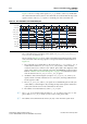
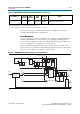
full-rate clock. Two types of addressing are possible:
■ 1T (full rate)—the duration of the address and command is a single memory clock
cycle (
mem_clk_2x
, Figure 5–6). This applies to all address and command signals in
full-rate designs or
mem_cs_n
,
mem_cke
, and
mem_odt
signals in half-rate designs.
■ 2T (half rate)—the duration of the address and command is two memory clock
cycles. For half-rate designs, the ALTMEMPHY megafunction supports only a
burst size of four, which means the burst size on the local interface is always set to
1. The size of the data is 4
n
-bits wide on the local side and is n-bits wide on the
memory side. To transfer all the 4n-bits at the double data rate, two memory-clock
cycles are required. The new address and command can be issued to memory
every two clock cycles. This scheme applies to all address and command signals,
except for
mem_cs_n
,
mem_cke
, and
mem_odt
signals in half-rate mode.
1 Refer to Table 5–1 on page 5–14 to see the frequency relationship of
mem_clk_2x
with
the rest of the clocks.