
User guide

5–20 Chapter 5: Functional Description—ALTMEMPHY
Block Description
External Memory Interface Handbook Volume 3 December 2010 Altera Corporation
Section II. DDR3 SDRAM Controller with ALTMEMPHY IP User Guide
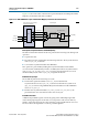
Read Data Alignment
Data alignment is the process controlled by the sequencer to ensure the correct
captured read data is present in the same half-rate clock cycle at the output of the read
data DPRAM. Data alignment is implemented using memory blocks in the core of
devices.
Postamble Protection
A dedicated postamble register controls the gating of the shifted DQS signal that
clocks the DQ input registers at the end of a read operation. Any glitches on the DQS
input signals at the end of the read postamble time do not cause erroneous data to be
captured as a result of postamble glitches. The postamble path is also calibrated to
determine the correct clock cycle, clock phase shift, and delay chain settings.
Stratix III and Stratix IV Devices
The DDR3 SDRAM controller asserts
ctl_doing_rd
to indicate that a read command
is requested. The
ctl_doing_rd
signal is then used for the following purposes:
■ Control of the postamble circuit
■ Generation of
ctl_rdata_valid
from one bit to two bits
■ Dynamic OCT control timing
The DDR3 SDRAM ALTMEMPHY then asserts the
ctl_rdata_valid
signal to
indicate that the data on the read data bus is valid. The
ctl_rdata_valid
signal is two
bits wide to allow controllers to issue reads and writes that are aligned to either the
half-cycle of the half-rate clock.
When calibration is over, the read latency of the PHY (the
ctl_rlat
signal) is sent
back to the controller to indicate how long it takes in
ctl_clk
clock cycles from
assertion of the
ctl_doing_read
signal to the valid read data returning on the
ctl_rdata
bus. The
ctl_rlat
signal is only valid when calibration has successfully
completed and never changes values during normal user mode operation.
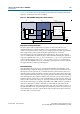
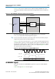
The read datapath for DDR3 SDRAM consists of two main blocks:
■ Read data capture, resynchronization, and demultiplexing (in the
dp_io_siii
module)
■ Read data alignment logic (in the
read_dp
module) to transfer data from the
resync_clk_2x
(half-rate resynchronization) clock domain to the
phy_clk
clock
domain.
As the DQS/DQSn signal is not continuous, the PHY also has postamble protection
logic to ensure that any glitches on the DQS input signals at the end of the read
postamble time do not cause erroneous data to be captured as a result of postamble
glitches.