
User guide

5–22 Chapter 5: Functional Description—ALTMEMPHY
Block Description
External Memory Interface Handbook Volume 3 December 2010 Altera Corporation
Section II. DDR3 SDRAM Controller with ALTMEMPHY IP User Guide
The postamble path is also calibrated to determine the correct clock cycle, clock phase
shift, and delay chain settings. You can see the process in simulation if you choose
Full calibration (long simulation time) mode in the MegaWizard Plug-In Manager.
Write Datapath
This topic discusses the write datapath.
Arria II GX Devices
The write datapath logic efficiently transfers data from the HDR memory controller to
DDR3 SDRAM. The write datapath logic consists of:
■ DQ and DQ output-enable logic
■ DQS/DQSn and DQS/DQSn output-enable logic
■ DM logic
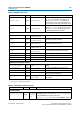
The memory controller interface outputs 4n-bit wide data (
ctl_wdata[4n]
) at half-rate
frequency. Figure 5-4 shows that the HDR write data (
ctl_wdata[4n]
) is clocked by
the half-rate clock
phy_clk_1x
(
ctl_clk
) and is converted into SDR, which is
represented by
wdp_wdata_h
and
wdp_wdata_l
and clocked by the full-rate clock
write_clk_2x
. The DQ IOEs convert 2-
n
SDR bits to
n
-DDR bits.
Stratix III and Stratix IV Devices
The memory controller interface outputs four n-bit wide data (
ctl_wdata
) at
phy_clk_1x
frequency. The write data is clocked by the system clock
phy_clk_1x
at
half-data rate (HDR) and reordered into HDR of width four with n-bits each,
represented in Figure 5–12 by
wdp_wdata3_1x
,
wdp_wdata2_1x
,
wdp_wdata1_1x
, and
wdp_wdata0_1x
.
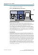
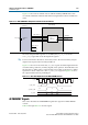
Figure 5–11. DDR3 SDRAM Write Datapath in Arria II GX Devices
Write Datapath
Arria II GX Device
wdp_wdata_l
phy_clk_1x
D
Q
D
Q
OE
DQ[n]
write_clk_2x
ctl_mem_wdata[4n]
write_clk_2x
Data
Multiplexing
wdp_wdata_h