
User guide

Chapter 5: Functional Description—ALTMEMPHY 5–33
PHY-to-Controller Interfaces
December 2010 Altera Corporation External Memory Interface Handbook Volume 3
Section II. DDR3 SDRAM Controller with ALTMEMPHY IP User Guide
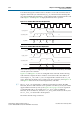
■ With the AFI, high and low signals are combined in one signal, so for a single chip
select (
ctl_cs_n
) interface,
ctl_cs_n[1:0]
, where location 0 appears on the
memory bus on one
mem_clk
cycle and location 1 on the next
mem_clk
cycle.
1 This convention is maintained for all signals so for an 8 bit memory
interface, the write data (
ctl_wdata
) signal is
ctl_wdata[31:0]
, where the
first data on the DQ pins is
ctl_wdata[7:0]
, then
ctl_wdata[15:8]
, then
ctl_wdata[23:16]
, then
ctl_wdata[31:24]
.
■ Word-aligned and word-unaligned reads and writes have the following
definitions:
■ Word-aligned for the single chip select is active (low) in location 1 (
_l
).
ctl_cs_n[1:0]
=
01
when a write occurs. This alignment is the easiest
alignment to design with.
■ Word-unaligned is the opposite, so
ctl_cs_n[1:0]
=
10
when a read or write
occurs and the other control and data signals are distributed across consecutive
ctl_clk
cycles.
1 The Altera high-performance controllers use word-aligned data only.
1 The timing analysis script does not support word-unaligned reads and
writes.
1 Word-unaligned reads and writes are only supported on Stratix III and
Stratix IV devices.
■ Spaced reads and writes have the following definitions:
■ Spaced writes—write commands separated by a gap of one controller clock
(
ctl_clk
) cycle
■ Spaced reads—read commands separated by a gap of one controller clock
(
ctl_clk
) cycle
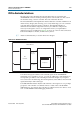
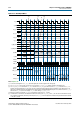
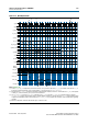
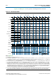
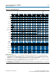
Figure 5–17 through Figure 5–20 assume the following general points:
■ The burst length is four. A DDR2 SDRAM is used—the interface timing is identical
for DDR3 devices.
■ An 8-bit interface with one chip select.
■ The data for one controller clock (
ctl_clk
) cycle represents data for two memory
clock (
mem_clk
) cycles (half-rate interface).