
User guide

5–34 Chapter 5: Functional Description—ALTMEMPHY
PHY-to-Controller Interfaces
External Memory Interface Handbook Volume 3 December 2010 Altera Corporation
Section II. DDR3 SDRAM Controller with ALTMEMPHY IP User Guide
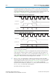
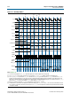
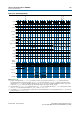
Figure 5–17. Word-Aligned Writes
Notes to Figure 5–17:
(1) To show the even alignment of
ctl_cs_n
, expand the signal (this convention applies for all other signals).
(2) The
ctl_dqs_burst
must go high one memory clock cycle before
ctl_wdata_valid
. Compare with the word-unaligned case.
(3) The
ctl_wdata_valid
is asserted two
ctl_wlat
controller clock (
ctl_clk
) cycles after chip select (
ctl_cs_n
) is asserted. The
ctl_wlat
indicates the required write latency in the system. The value is determined during calibration and is dependant upon the relative delays in the
address and command path and the write datapath in both the PHY and the external DDR SDRAM subsystem. The controller must drive
ctl_cs_n
and then wait
ctl_wlat
(two in this example)
ctl_clks
before driving
ctl_wdata_valid
.
(4) Observe the ordering of write data (
ctl_wdata
). Compare this to data on the
mem_dq
signal.
(5) In all waveforms a command record is added that combines the memory pins
ras_n
,
cas_n
and
we_n
into the current command that is issued.
This command is registered by the memory when chip select (
mem_cs_n
) is low. The important commands in the presented waveforms are WR
= write, ACT = activate.
ctl_clk
(4)( 2)(1)
ctl_wlat
ctl_ras_n
ctl_cas_n
ctl_we_n
ctl_cs_n
ctl_dqs_burst
ctl_wdata_valid
ctl_wdata
ctl_addr
Memory
Interface
mem_clk
command
(Note 5)
mem_cs_n
mem_dqs
mem_dq
(3)
00 00 11
2
11
11 00
1111 00
11
11 01 11 01 11
00
00 10 11 10 11 00
00
00 11 00 11
00000000 00000000 03020100 07060504 0b0a0908 0f0e0d0c
00000000
00000000 0020008
ACTACT WR