
User guide


5–40 Chapter 5: Functional Description—ALTMEMPHY
Using a Custom Controller
External Memory Interface Handbook Volume 3 December 2010 Altera Corporation
Section II. DDR3 SDRAM Controller with ALTMEMPHY IP User Guide
The ALTMEMPHY provides a signal,
ctl_rdata_valid
, to indicate that the data on
read data bus is valid. The width of this signal varies between half-rate and full-rate
designs to support the option to indicate that the read data is not word aligned.
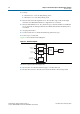
Figure 5–21 and Figure 5–22 show these relationships.
Handshake Mechanism Between Write Commands and Write Data
In the AFI, the ALTMEMPHY output
ctl_wlat
gives the number of
ctl_clk
cycles
between the write command that is issued
ctl_cs_n
asserted and
ctl_dqs_burst
asserted. The
ctl_wlat
signal considers the following actions to provide a single
value in
ctl_clk
clock cycles:
■ CAS write latency
■ Additive latency
■ Datapath latencies and relative phases
■ Board layout
■ Address and command path latency and
1T
register setting, which is dynamically
setup to take into account any leveling effects
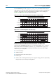
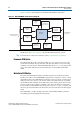
Figure 5–21. Address and Command and Read-Path Timing—Full-Rate Design
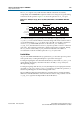
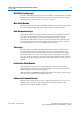
Figure 5–22. Second Read Alignment—Half-Rate Design
ctl_clk
ctl_addr
ctl_cs_n
ctl_doing_read
mem_dqs
mem_dq
ctl_rdata_valid
ctl_rdata
ctl_rlat = 9
1 2 3 4 5 6 7 8 9
ctl_clk
1 2 3 4 5 6 7
8 9
ctl_rlat = 9
ctl_addr
ctl_cs_n
ctl_doing_read
mem_dqs
mem_dq
ctl_rdata_valid
ctl_rdata
A XA
1010
10 0101
10 0101
DX XD