
User guide


6–2 Chapter 6: Functional Description—High-Performance Controller
Block Description
External Memory Interface Handbook Volume 3 December 2010 Altera Corporation
Section II. DDR3 SDRAM Controller with ALTMEMPHY IP User Guide
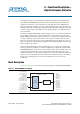
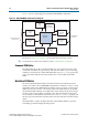
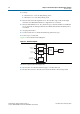
Figure 6–2 shows a block diagram of the DDR3 SDRAM HPC architecture.
The blocks in Figure 6–2 on page 6–2 are described in the following sections.
f For information on the Avalon interface, refer to Avalon Interface Specifications.
Command FIFO Buffer
This FIFO buffer allows the controller to buffer up to four consecutive read or write
commands. It is built from logic elements, and stores the address, read or write flag,
and burst count information. If this FIFO buffer fills up, the
local_ready
signal to the
user is deasserted until the main state machine takes a command from the FIFO
buffer.
Write Data FIFO Buffer
The write data FIFO buffer holds the write data from the user until the main state
machine can send it to the ALTMEMPHY megafunction, which does not have a write
data buffer. In the Avalon-MM interface mode, the user logic presents a write request,
address, burst count, and one or more beats of data. The write data beats are placed
into the FIFO buffer until they are needed. In the native interface mode, the user logic
presents a write request, address, and burst count. The controller then requests the
correct number of write data beats from the user via the
local_wdata_req
signal, and
the user logic must return the write data in the clock cycle after the write data request
signal.
This FIFO buffer is sized to be deeper than the command FIFO buffer to prevent it
from filling up and interrupting streaming writes.
Figure 6–2. DDR3 SDRAM HPC Architecture Block Diagram
Timer
Logic
Initialization
State Machine
Command
FIFO
ALTMEMPHY
Interface
Avalon-MM or Native
Slave Interface
Write Data
FIFO
Bank
Management
Logic
Write Data
Tracking Logic
Address and
Command
Decode
PHY Interface
Logic
Main State
Machine