
User guide


2–6 Altera Corporation
Stratix GX Transceiver User Guide January 2005
Transmitter Analog
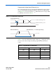
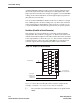
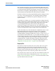
Figure 2–4. Transmitter PLL Block Diagram
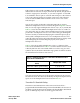
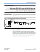
Table 2–2 lists some of the transmitter PLL specifications.
Clock Synthesis
The maximum input frequency of the phase frequency detector (PFD) is
325 MHz. To achieve reference clock frequency above this limitation, the
/2 pre-divider on the dedicated local REFCLKB path can be enabled
automatically by the Quartus
®
II software. The /2 pre-divider divides the
reference clock frequency by a factor of 2 and then the /m factor
compensates the frequency difference. An example would be a data rate
of 2,488 Mbps with a 622-MHz reference clock. In this scenario, the
reference clock must be assigned to the REFCLKB port where the 622-
MHz reference clock is divided by 2, yielding a 311-MHz clock at the PFD.
This 311-MHz reference clock is then multiplied by a factor of 8 to achieve
the 2,488-MHz clock at the VCO.
/2
Inter Quad Routing (IQ1)
Inter Quad Routing (IQ0)
Global Clocks, I/O Bus, General Routing
Dedicated Local
REFCLKB
PFD CP+LF
Up
DownINCLK
VCO
/m
Clock
Driver
High Speed
TX_PLL_CLK
Low Speed
TX_PLL_CLK
/4, 8, 10, 16, 20
Table 2–2. Transmitter PLL Specifications
Parameter Specifications
Input reference frequency range 25 MHz to 650 MHz
Data rate support 500 Mbps to 3.1875 Gbps
Multiplication factor (W) 2, 4, 5, 8, 10, 16, or 20 (1)
Note to Ta b le 2 – 2:
(1) Multiplication factors 2 and 5 can only be achieved with the use of the pre-divider
on the REFCLKB.