
User guide

4–12 Altera Corporation
Stratix GX Transceiver User Guide January 2005
SONET Mode Clocking
The Transmitter Phase Compensation FIFO module is always used and
cannot be bypassed. The input to the Transmitter Phase Compensation
FIFO module is the data from the FPGA logic array.
Byte Serializer
In SONET mode, the Byte Serializer in the transmitter block takes in a
16-bit input from the phase compensation FIFO module and serializes it
to 8 bits. It transmits the least significant byte to the most significant byte.
The transmitter digital reset must always be used to reset the Byte
Serializer FIFO module pointers whenever an unknown state is
encountered, for example, during periods when the transmitter PLL loses
lock. Refer to Chapter 8, Reset Control and Power Down, for further
details on the reset sequence.
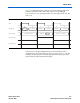
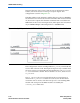
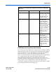
Figure 4–10 demonstrates input and output signals of the byte serializer
when serializing a 16 bit input to 8 bits. The tx_in[] signal is the
input from the FPGA logic array that has already passed through the
Transmitter Phase Compensation FIFO module.
Figure 4–10. Transmitter Byte Serializer in 8- to 16-Bit Mode
The LSB is transmitted before the MSB in the transmitter byte serializer.
Figure 4–10 shows the order of data transmitted. For the input of D1, the
output is D1LSB and then D1MSB. The byte serializer is selected in the
MegaWizard Plug-In Manager when a 16-bit channel width is selected.
SONET Mode
Clocking
SONET Mode Channel Clocking
This section covers describes the internal clocking and the external clocks
of the transceiver in SONET mode. By default, the MegaWizard Plug-In
Manager parameterizes the altgxb megafunction with the clock
configuration shown in Figure 4–11.
datain[15..0]
D1
dataout[7..0]
D2 D3
MSBLSB
D1
LSB MSB
D2
0001010001101111
xxxxxxxx 01101111xxxxxxxx 00010100 1100011011110001
1100011011110001 1010101010110011