
User guide

Altera Corporation 4–17
January 2005 Stratix GX Transceiver User Guide
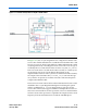
SONET Mode
SONET Mode Inter-Transceiver Block Clocking
This section provides guidelines for using transceiver interface clocking
between the FPGA logic array and transceiver channels when multiple
transceiver blocks are active. Depending on each mode supported by
Stratix GX devices, each transceiver block contains different
transceiver-to-FPGA interface clocking. Different input and output clocks
are available based on the options provided by the Quartus II
MegaWizard Plug-In Manager’s built-in functions. The number of
supported channels varies based on which Stratix GX device you select.
Because of the various configurations of input and output clocks,
consider the clocking schemes between inter-transceiver blocks carefully
to prevent problems later in the design cycle.
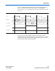
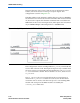
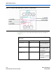
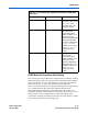
rx_clkout
Output Output clock from
transceiver. In this mode,
rx_clkout is the
recovered clock of the
respective channel.
tx_coreclk
Input Clocks the write port of
transmitter phase
compensation FIFO
module. Available as an
optional port in the
Quartus II MegaWizard®
Plug-In Manager. Must
be frequency matched to
tx_pll_clk. If not
available as a port, this is
fed by
coreclk_out
through logic array
routing.
rx_coreclk
Input Clocks read port of
receiver phase
compensation FIFO
module. Available as an
optional port in the
Quartus II MegaWizard
Plug-In Manager. If not
available as a port, this is
fed by
rx_clkout
through logic array
routing.
Table 4–2. List of Clocking Input & Output Ports Available in SONET Mode
(Part 2 of 2)
Clock Port Description