
Specifications


Chapter 2: Board Components 2–11
MAX V CPLD System Controller
October 2014 Altera Corporation Stratix V GX FPGA Development Board
Reference Manual
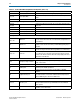
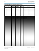
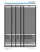
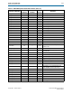
MAX5_BEN1
R11 T31 1.8-V MAX V byte enable 1
MAX5_BEN2
T12 N33 1.8-V MAX V byte enable 2
MAX5_BEN3
N11 M33 1.8-V MAX V byte enable 3
MAX5_CLK
T11 E34 1.8-V MAX V clock
MAX5_CSN
R10 B32 1.8-V MAX V chip select
MAX5_OEN
M10 A32 1.8-V MAX V output enable
MAX5_WEN
N10 A34 1.8-V MAX V write enable
MAX_CONF_DONE
E11 — 1.8-V FPGA configuration done LED
MAX_ERROR
A4 — 1.8-V FPGA configuration error LED
MAX_LOAD
A6 — 1.8-V FPGA configuration active LED
MAX_RESETn
M9 — 1.8-V MAX V reset push button
MSEL0
B10 AA9 2.5-V DIP switch for FPGA mode select 0
MSEL1
B3 AA10 2.5-V DIP switch for FPGA mode select 1
MSEL2
C10 AD8 2.5-V DIP switch for FPGA mode select 2
MSEL3
C12 AG8 2.5-V DIP switch for FPGA mode select 3
MSEL4
C6 AH7 2.5-V DIP switch for FPGA mode select 4
OVERTEMP
B7 — 2.5-V Temperature monitor fan enable
OVERTEMPn
C8 — 2.5-V
Temperature monitor over-temperature
indicator LED
PCIE_JTAG_EN
C7 — 2.5-V DIP switch to enable the PCIe JTAG master
PGM_CONFIG
D12 — 2.5-V
Loads the flash memory image identified by
the PGM LEDs
PGM_LED0
B14 — 2.5-V Flash memory PGM select indicator 0
PGM_LED1
C13 — 2.5-V Flash memory PGM select indicator 1
PGM_LED2
B16 — 2.5-V Flash memory PGM select indicator 2
PGM_SEL
B13 — 2.5-V Toggles the
PGM_LED[0:2]
sequence
SDI_RX_BYPASS
D5 AB30 2.5-V SDI equalization bypass
SDI_RX_EN
E8 AB28 2.5-V SDI receive enable
SDI_TX_EN
D11 AK27 2.5-V SDI transmit enable
SECURITY_MODE
R12 — 1.8-V
DIP switch for on-board USB-Blaster II to
send FACTORY command at power up.
SENSE_CS0n
E7 — 2.5-V Power monitor chip select
SENSE_SCK
A5 — 2.5-V Power monitor SPI clock
SENSE_SDI
D7 — 2.5-V Power monitor SPI data in
SENSE_SDO
B6 — 2.5-V Power monitor SPI data out
SENSE_SMB_CLK
D8 — 2.5-V Temperature monitor SMB clock
SENSE_SMB_DATA
A7 — 2.5-V Temperature monitor SMB data
SI570_EN
A10 — 2.5-V Si570 programmable oscillator enable
Table 2–5. MAX V CPLD System Controller Device Pin-Out (Part 5 of 6)
Schematic Signal Name
MAX V CPLD
Pin Number
Stratix V GX FPGA
Pin Number
I/O
Standard
Description