
Specifications


2–26 Chapter 2: Board Components
General User Input/Output
Stratix V GX FPGA Development Board October 2014 Altera Corporation
Reference Manual
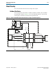
Memory Clocks
The development board includes memory clocks which are driven to or received from
the on-board memory devices. For more information on the memory clock signals,
refer to the section on “Memory” on page 2–46.
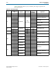
Table 2–25 lists the crystal oscillators component references and manufacturing
information.
General User Input/Output
This section describes the user I/O interface to the FPGA. This section describes the
following I/O elements:
■ User-defined push buttons
■ User-defined DIP switch
■ User-defined LEDs
■ Character LCD
User-Defined Push Buttons
The development board includes three user-defined push buttons. Board references
S5, S6, and S7 are push buttons that allow you to interact with the Stratix V GX FPGA
device. When you press and hold down the push button, the device pin is set to logic
0; when you release the push button, the device pin is set to logic 1. There is no
board-specific function for these general user push buttons.
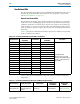
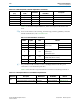
Table 2–25. Crystal Oscillator Component References and Manufacturing Information
Board
Reference
Description Manufacturer
Manufacturer
Part Number
Manufacturer Website
X1
148.50 MHz LVDS voltage
controlled crystal oscillator
Epson
EG-2121CA
125.0000M-LGPNL3
www.eea.epson.com
X2 100 MHz 2.5-V CMOS oscillator ECS, Inc. ECS-3525-1000-B-TR www.ecsxtal.com
X3 50 MHz 1.8-V oscillator ECS, Inc. ECS-3518-500-B-xx www.ecsxtal.com
X4
100.00 MHz LVDS
programmable crystal oscillator
Silicon Labs 570FAB000433DG www.silabs.com
X6 125 MHz LVDS saw oscillator Silicon Labs 571FDB000159DG www.silabs.com
U38
Programmable LVDS
quad-clock 100M, 156.25M,
625M, 270M defaults
Silicon Labs Si5338A-A01086-GM www.silabs.com
U46
Programmable LVDS
quad-clock 125M, 644.53125M,
282.5M, 125M defaults
Silicon Labs Si5338A-A01085-GM www.silabs.com