
Specifications

2–40 Chapter 2: Board Components
Components and Interfaces
Stratix V GX FPGA Development Board October 2014 Altera Corporation
Reference Manual
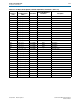
Table 2–41 lists the HSMC port B interface pin assignments, signal names, and
functions.
Table 2–41. HSMC Port B Pin Assignments, Schematic Signal Names, and Functions (Part 1 of 3)
Board
Reference
(J2)
Schematic Signal Name I/O Standard
Stratix V GX FPGA
Device Pin Number
Description
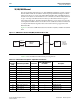
30
HSMB_RX_P0
1.4-V PCML F2 Transceiver receive channel
32
HSMB_RX_N0
1.4-V PCML F1 Transceiver receive channel
26
HSMB_RX_P1
1.4-V PCML D2 Transceiver receive channel
28
HSMB_RX_N1
1.4-V PCML D1 Transceiver receive channel
22
HSMB_RX_P2
1.4-V PCML Y2 Transceiver receive channel
24
HSMB_RX_N2
1.4-V PCML Y1 Transceiver receive channel
18
HSMB_RX_P3
1.4-V PCML V2 Transceiver receive channel
20
HSMB_RX_N3
1.4-V PCML V1 Transceiver receive channel
29
HSMB_TX_P0
1.4-V PCML E4 Transceiver transmit channel
31
HSMB_TX_N0
1.4-V PCML E3 Transceiver transmit channel
25
HSMB_TX_P1
1.4-V PCML C4 Transceiver transmit channel
27
HSMB_TX_N1
1.4-V PCML C3 Transceiver transmit channel
21
HSMB_TX_P2
1.4-V PCML W4 Transceiver transmit channel
23
HSMB_TX_N2
1.4-V PCML W3 Transceiver transmit channel
17
HSMB_TX_P3
1.4-V PCML U4 Transceiver transmit channel
19
HSMB_TX_N3
1.4-V PCML U3 Transceiver transmit channel
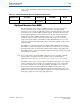
158
HSMB_CLK_IN_N2
LVDS or 2.5-V N16 LVDS or CMOS clock in 2
96
HSMB_CLK_IN_P1
LVDS or 2.5-V U15 Secondary differential clock in
156
HSMB_CLK_IN_P2
LVDS or 2.5-V P16 Primary source-synchronous clock in
39
HSMB_CLK_OUT0
LVDS or 2.5-V L16 Primary single-ended clock out
97
HSMB_CLK_OUT_N1
LVDS or 2.5-V C16 LVDS or CMOS clock out 1
157
HSMB_CLK_OUT_N2
LVDS or 2.5-V A16 LVDS or CMOS clock out 2
95
HSMB_CLK_OUT_P1
LVDS or 2.5-V D16 Secondary differential clock out
155
HSMB_CLK_OUT_P2
LVDS or 2.5-V B16 Primary source-synchronous clock out
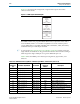
50
HSMB_A0
2.5-V CMOS N17 Memory address bit
54
HSMB_A1
2.5-V CMOS P17 Memory address bit
56
HSMB_A2
2.5-V CMOS H13 Memory address bit
60
HSMB_A3
2.5-V CMOS G14 Memory address bit
62
HSMB_A4
2.5-V CMOS L18 Memory address bit
74
HSMB_A5
2.5-V CMOS L19 Memory address bit
78
HSMB_A6
2.5-V CMOS K19 Memory address bit
80
HSMB_A7
2.5-V CMOS J18 Memory address bit
84
HSMB_A8
2.5-V CMOS A17 Memory address bit
86
HSMB_A9
2.5-V CMOS B17 Memory address bit
104
HSMB_A10
2.5-V CMOS G18 Memory address bit
108
HSMB_A11
2.5-V CMOS C18 Memory address bit