
Specifications


Chapter 2: Board Components 2–47
Memory
October 2014 Altera Corporation Stratix V GX FPGA Development Board
Reference Manual
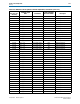
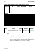
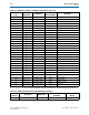
Table 2–50 lists the DDR3 devices pin assignments, signal names, and functions.
Table 2–50. DDR3 Devices Pin Assignments, Schematic Signal Names, and Functions (Part 1 of 4)
Board Reference
(U12, U17, U21,
U23, U28)
Schematic Signal
Name
I/O Standard
Stratix V GX FPGA
Device Pin Number
Description
DDR3 x16 / DDR3 x8 pins
T3
DDR3_A13
1.5-V SSTL Class I J31 Address bus
N7
DDR3_A12
1.5-V SSTL Class I R30 Address bus
R7
DDR3_A11
1.5-V SSTL Class I L31 Address bus
L7
DDR3_A10
1.5-V SSTL Class I J30 Address bus
R3
DDR3_A9
1.5-V SSTL Class I J29 Address bus
T8
DDR3_A8
1.5-V SSTL Class I P31 Address bus
R2
DDR3_A7
1.5-V SSTL Class I F30 Address bus
R8
DDR3_A6
1.5-V SSTL Class I N31 Address bus
P2
DDR3_A5
1.5-V SSTL Class I E31 Address bus
P8
DDR3_A4
1.5-V SSTL Class I L30 Address bus
N2
DDR3_A3
1.5-V SSTL Class I D31 Address bus
P3
DDR3_A2
1.5-V SSTL Class I H31 Address bus
P7
DDR3_A1
1.5-V SSTL Class I K31 Address bus
N3
DDR3_A0
1.5-V SSTL Class I G31 Address bus
M3
DDR3_BA2
1.5-V SSTL Class I E30 Bank address bus
N8
DDR3_BA1
1.5-V SSTL Class I K30 Bank address bus
M2
DDR3_BA0
1.5-V SSTL Class I C31 Bank address bus
T2
DDR3_RESETn
1.5-V SSTL Class I G30 Reset
J3
DDR3_RASn
1.5-V SSTL Class I B26 Row address select
K3
DDR3_CASn
1.5-V SSTL Class I B28 Column address select
L2
DDR3_CSn
1.5-V SSTL Class I B31 Chip select
L3
DDR3_WEn
1.5-V SSTL Class I C30 Write enable
K1
DDR3_ODT
1.5-V SSTL Class I A31 On-die termination enable
L8
DDR3_ZQ
1.5-V SSTL Class I — ZQ impedance calibration
K9
DDR3_CKE
1.5-V SSTL Class I R31 Clock enable
J7
DDR3_CLK_P
1.5-V SSTL Class I N30 Differential output clock
K7
DDR3_CLK_N
1.5-V SSTL Class I M30 Differential output clock
DDR3 x16 pins
U28.E3
DDR3_DQ0
1.5-V SSTL Class I A28 Data bus byte lane 0
U28.F7
DDR3_DQ1
1.5-V SSTL Class I E28 Data bus byte lane 0
U28.F2
DDR3_DQ2
1.5-V SSTL Class I B29 Data bus byte lane 0
U28.F8
DDR3_DQ3
1.5-V SSTL Class I F29 Data bus byte lane 0
U28.H3
DDR3_DQ4
1.5-V SSTL Class I D28 Data bus byte lane 0
U28.H8
DDR3_DQ5
1.5-V SSTL Class I H28 Data bus byte lane 0
U28.G2
DDR3_DQ6
1.5-V SSTL Class I C28 Data bus byte lane 0