
Specifications


2–50 Chapter 2: Board Components
Memory
Stratix V GX FPGA Development Board October 2014 Altera Corporation
Reference Manual
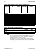
Table 2–51 lists the DDR3 component reference and manufacturing information.
QDRII+
The development board supports a burst-of-4 QDRII+ SRAM memory device for
very-high-speed, low-latency memory access. The QDRII+ has a x18 interface,
providing addressing to a device of up to a 32 Mb.
The QDRII+ has separate read and write data ports with DDR signaling at up to
550 MHz. The pinout and footprint is compatible with a burst-of-2 QDRII SSRAM
memory device. Although the FPGA supports up to 350 MHz QDRII data, the fastest
RoHS compliant QDRII device being manufactured is only 333 MHz.
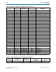
U17.B8
DDR3_DQ62
1.5-V SSTL Class I G20 Data bus byte lane 7
U17.A3
DDR3_DQ63
1.5-V SSTL Class I E20 Data bus byte lane 7
U17.D3
DDR3_DM7
1.5-V SSTL Class I B20 Write mask byte lane 7
U17.C7
DDR3_DQS_P7
1.5-V SSTL Class I G21 Data strobe P byte lane 7
U17.B7
DDR3_DQS_N7
1.5-V SSTL Class I F21 Data strobe N byte lane 7
DDR3 x8 pins
U12.B3
DDR3_DQ64
1.5-V SSTL Class I M20 Data bus byte lane 8
U12.C7
DDR3_DQ65
1.5-V SSTL Class I L20 Data bus byte lane 8
U12.C2
DDR3_DQ66
1.5-V SSTL Class I N22 Data bus byte lane 8
U12.C8
DDR3_DQ67
1.5-V SSTL Class I J21 Data bus byte lane 8
U12.E3
DDR3_DQ68
1.5-V SSTL Class I N21 Data bus byte lane 8
U12.E8
DDR3_DQ69
1.5-V SSTL Class I K21 Data bus byte lane 8
U12.D2
DDR3_DQ70
1.5-V SSTL Class I N20 Data bus byte lane 8
U12.E7
DDR3_DQ71
1.5-V SSTL Class I L21 Data bus byte lane 8
U12.B7
DDR3_DM8
1.5-V SSTL Class I M21 Write mask byte lane 8
U12.C3
DDR3_DQS_P8
1.5-V SSTL Class I K22 Data strobe P byte lane 8
U12.D3
DDR3_DQS_N8
1.5-V SSTL Class I J22 Data strobe N byte lane 8
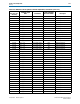
Table 2–50. DDR3 Devices Pin Assignments, Schematic Signal Names, and Functions (Part 4 of 4)
Board Reference
(U12, U17, U21,
U23, U28)
Schematic Signal
Name
I/O Standard
Stratix V GX FPGA
Device Pin Number
Description
Table 2–51. DDR3 Component Reference and Manufacturing Information
Board
Reference
Description Manufacturer
Manufacturing
Part Number
Manufacturer
Website
U17, U21,
U23, U28
16 M × 16-bit × 8 banks, 800 MHz, CL11 Micron MT41J128M16HA-125 www.micron.com
U12 16 M × 8-bit × 8 banks, 800 MHz, CL11 Micron MT41J128M8JP-125 www.micron.com