
Specifications


Chapter 2: Board Components 2–53
Memory
October 2014 Altera Corporation Stratix V GX FPGA Development Board
Reference Manual
RLDRAM II
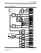
The development board supports a 32Mx18x8 bank CIO RLDRAM II SRAM interface
for very-high-speed sequential memory access. The 18-bit data bus comprises of a
single x18 device with a single address or command bus. This interface connects to the
vertical I/O banks on the bottom edge of the FPGA. The target speed is 533 MHz.
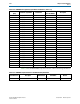
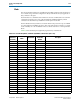
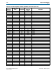
Table 2–54 lists the RLDRAM II pin assignments, signal names, and functions.
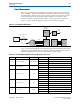
Table 2–54. RLDRAM II Pin Assignments, Signal Names and Functions (Part 1 of 2)
Board Reference
(U20)
Schematic Signal Name I/O Standard
Stratix V GX FPGA
Device Pin Number
Description
G12
RLDC_A0
1.8-V HSTL Class I AD22 Address bus
G11
RLDC_A1
1.8-V HSTL Class I AW22 Address bus
G10
RLDC_A2
1.8-V HSTL Class I AW23 Address bus
H12
RLDC_A3
1.8-V HSTL Class I AD23 Address bus
H11
RLDC_A4
1.8-V HSTL Class I AE22 Address bus
F1
RLDC_A5
1.8-V HSTL Class I AU23 Address bus
G2
RLDC_A6
1.8-V HSTL Class I AT23 Address bus
G3
RLDC_A7
1.8-V HSTL Class I AT20 Address bus
G1
RLDC_A8
1.8-V HSTL Class I AG23 Address bus
H2
RLDC_A9
1.8-V HSTL Class I AM23 Address bus
M12
RLDC_A10
1.8-V HSTL Class I AM20 Address bus
M11
RLDC_A11
1.8-V HSTL Class I AW20 Address bus
M10
RLDC_A12
1.8-V HSTL Class I AV20 Address bus
L12
RLDC_A13
1.8-V HSTL Class I AG22 Address bus
L11
RLDC_A14
1.8-V HSTL Class I AF23 Address bus
P1
RLDC_A15
1.8-V HSTL Class I AR21 Address bus
M2
RLDC_A16
1.8-V HSTL Class I AP22 Address bus
M3
RLDC_A17
1.8-V HSTL Class I AR20 Address bus
N1
RLDC_A18
1.8-V HSTL Class I AR22 Address bus
N12
RLDC_A19
1.8-V HSTL Class I AN20 Address bus
E12
RLDC_A20
1.8-V HSTL Class I AU20 Address bus
E1
RLDC_A21
1.8-V HSTL Class I AV23 Address bus
D1
RLDC_A22
1.8-V HSTL Class I AV22 Address bus
J11
RLDC_BA0
1.8-V HSTL Class I AE23 Bank address bus
K11
RLDC_BA1
1.8-V HSTL Class I AF22 Bank address bus
H1
RLDC_BA2
1.8-V HSTL Class I AK23 Bank address bus
K12
RLDC_CK_N
1.8-V HSTL Class I AU21 Input clock
J12
RLDC_CK_P
1.8-V HSTL Class I AT21 Input clock
L2
RLDC_CSN
1.8-V HSTL Class I AN23 Chip select
K2
RLDC_DK_N
1.8-V HSTL Class I AR25 Data clock
K1
RLDC_DK_P
1.8-V HSTL Class I AP25 Data clock
P12
RLDC_DM
1.8-V HSTL Class I AB25 Data mask