
Specifications


Chapter 2: Board Components 2–59
Power Supply
October 2014 Altera Corporation Stratix V GX FPGA Development Board
Reference Manual
Power Measurement
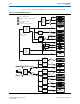
There are 16 power supply rails which have on-board voltage, current, and wattage
sense capabilities. These 8-channel differential 24-bit ADC devices and rails are split
from the primary supply plane by a low-value sense resistor for the ADC to measure
voltage and current. A serial peripheral interface (SPI) bus connects these ADC
devices to the MAX V CPLD System Controller as well as the Stratix V GX FPGA.
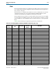
Figure 2–11 shows the block diagram for the power measurement circuitry.
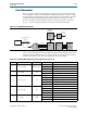
Table 2–59 lists the targeted rails. The schematic signal name specifies the name of the
rail being measured and the device pin specifies the devices attached to the rail. If no
subnet is named, the power is the total output power for that voltage.
Figure 2–11. Power Measurement Circuit
SCK
DSI
DSO
CSn
8 Ch.
Power Supply Load 0-7
Supply
0-7
R
SENSE
5M2210
5GXA7
LTC2418
EPM570G
USB
PHY
To User PC
Power GUI
JTAG Chain
SPI Bus
On-Board
USB-Blaster II
Feedback
14-pin
2x16
Character LCD
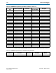
Table 2–59. Power Rail Measurements Based on the GUI Selection (Part 1 of 2)
Number Schematic Signal Name Voltage (V) Device Pin Description
0
S5_VCCIO_HSMB
1.2/1.5/1.8/2.5
VCCIO_7A I/O supply bank 7A
VCCIO_7C I/O supply bank 7C (HSMC Port B)
VCCIO_7D I/O supply bank 7D (HSMC Port B)
1
S5_VCC_GXB
1.1
VCCR_GXB XCVR analog receive
VCCT_GXB XCVR analog transmit
2
S5_VCCIO_1.8V
1.8
VCCIO_3C I/O supply bank 3C (RLDRAM II)
VCCIO_3D I/O supply bank 3D (RLDRAM II)
VCCIO_4A I/O supply bank 4A
VCCIO_4C I/O supply bank 4C (QDR II/+)
VCCIO_4D I/O supply bank 4D (QDR II/+)
3
S5_VCCPD_PGM
2.5
VCCPD I/O pre-drivers
VCCPGM Configuration I/O
VCCAUX Programmable power tech auxiliary
VCCA_FPLL PLL analog power
4
S5_VCCINT
0.90
VCC FPGA core and periphery power
VCCHIP PCIe Hard IP digital power
VCCHSSI PCS power