
User guide


6–24 Chapter 6: Board Test System
The Clock Control
Stratix V GX FPGA Development Kit December 2014 Altera Corporation
User Guide
The Clock Control application runs as a stand-alone application. ClockControl.exe
resides in the
<install dir>\kits\stratixVGX_5sgxea7kf40_fpga\examples\board_test_system
directory. On Windows, click Start > All Programs > Altera > Stratix V GX FPGA
Development Kit <version> > Clock Control to start the application.
f For more information about the Si570, Si571, or Si5338 oscillators and the Stratix V GX
FPGA development board’s clocking circuitry and clock input pins, refer to the
Stratix V GX FPGA Development Board Reference Manual.
The Clock Control communicates with the MAX V device on the board through the
JTAG bus. The Si570, Si571, Si5338 (U38, U46) programmable oscillators are connected
to the MAX V device through a 2-wire serial bus. Clock frequencies will return to the
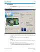
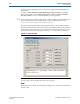
default values after power cycling the board. Figure 6–11 shows the Clock Control.
The following sections describe the Clock Control controls.
Read
The read control reads the current frequency setting for the oscillator associated with
the active tab.
Figure 6–11. The Clock Control