
User guide


Altera Corporation 43
101 Innovation Drive
San Jose, CA 95134
(408) 544-7000
www.altera.com
Applications Hotline:
(800) 800-EPLD
Literature Services:
lliterature@altera.com
Copyright © 2005 Altera Corporation. All rights reserved. Altera, The Programmable Solutions Company,
the stylized Altera logo, specific device designations, and all other words and logos that are identified as
trademarks and/or service marks are, unless noted otherwise, the trademarks and service marks of Altera
Corporation in the U.S. and other countries. All other product or service names are the property of their re-
spective holders. Altera products are protected under numerous U.S. and foreign patents and pending
applications, maskwork rights, and copyrights. Altera warrants performance of its semiconductor products
to current specifications in accordance with Altera's standard warranty, but reserves the right to make chang-
es to any products and services at any time without notice. Altera assumes no responsibility or liability
arising out of the application or use of any information, product, or service described
herein except as expressly agreed to in writing by Altera Corporation. Altera customers
are advised to obtain the latest version of device specifications before relying on any pub-
lished information and before placing orders for products or services.
Troubleshooting
Troubleshooting
This section contains the following troubleshooting questions and
solutions.
Why do I get errors when I load the Simulink design
filter_design.mdl?
In order to load the filter_design.mdl successfully, you must have the
correct versions of the DSP Builder, MATLAB/Simulink, and IP cores.
Refer to the section “Before You Begin” on page 3 for details.
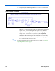
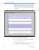
Why is my SignalTap II filtered signal different from the one
Figure 30 shows?
If the SMA cable is not securely connected between DAC CHANNEL A
and ADC CHANNEL A, you will not see a signal at the output of the FIR
filter during SignalTap II analysis. Ensure the correct settings for the
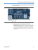
jumpers J30, J35 and J37, as specified in “Set Up the Stratix II EP2S180 DSP
Development Board for Hardware Analysis” on page 30. Figure 25 on
page 33 shows the jumper settings.
Conclusion
The Stratix II Professional filtering lab design provides a basic design
example using the on-board A/D converter and the on-board D/A
converter. It demonstrates SignalTap II analysis as a real-time FPGA
signal acquisition feature in the DSP Builder environment of Simulink.