PCB Design Training Module
Software, documentation and related materials: Copyright © 2006 Altium Limited. All rights reserved. You are permitted to print this document provided that (1) the use of such is for personal use only and will not be copied or posted on any network computer or broadcast in any media, and (2) no modifications of the document is made.
PCB Design Training Module 1. PCB design process ................................................................................................. 4-1 1. The PCB Editor workspace ...................................................................................... 4-3 1.1 PCB Panel ...................................................................................................... 4-3 1.2 Using the PCB Editor panel to browse........................................................... 4-4 1.
8.1 8.2 Interactive routing......................................................................................... 4-61 Automatic routing ......................................................................................... 4-67 9. Polygons .................................................................................................................. 4-69 9.1 Placing polygons .......................................................................................... 4-69 9.
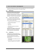
1. PCB design process The PCB Design training day covers how to use the PCB Editor to create a PCB from setup, through component placement, routing, design rule checking and CAM output. This first section looks at the overall PCB design process. The diagram below shows an overview of the PCB design process from schematic entry through to PCB design completion. Figure 1.
Once the PCB design is completed and verified, the Create Manufacturing Output process is used to generate the PCB output files. This process is outlined below in Figure 2. Figure 2.
2. The PCB Editor workspace This section investigates how to browse through a PCB design and how to set up the workspace preferences and other document options, such as layers and grids. 2.1 PCB Panel The PCB panel provides a powerful method of examining the contents of the PCB workspace. Clicking on an entry in the panel will filter the workspace to highlight that object – the highlighting will depend on the settings of the options at the top of the panel. To begin with, enable all the options. 2.1.
2.2 2.2.1 Using the PCB Editor panel to browse Browsing nets and net classes • To browse nets, select Nets from the dropdown list in the PCB panel. • Click on All Nets in the Net Classes region of the dialog to browse all nets on the PCB. The nets are listed in the region below and they are also highlighted on the PCB. • If the design includes Net Classes these are also listed. Net classes such as D[0..7] have been generated automatically from busses in the design.
2.2.2 Browsing components and component classes • To browse components, select Components from the drop-down list. • When the panel is being used to filter (highlight) components, you might find it better to have the Select option at the top of the panel switched off. • Click on All Components in the Components Class region to browse all components on the PCB. The components are listed in the Components region, as well as being highlighted on the display.
2.2.3 Browsing design rules and rule violations To browse design rules, select Rules from the drop-down list. All Rules classes are listed. • Click on a Rule Class and all rules defined for that class are listed in the Rules list. • Click on a rule in the Rules list to highlight all objects targeted by that rule. • Double-click on the rule to display a dialog to edit that rule. • If the selected rule is in violation, all violating objects are listed in the Violations region.
2.2.4 From-To editor • Choose From-To Editor from the drop-down field at the top of the PCB panel. The top list section of the panel will fill with all nets currently defined for the design. • As you click on a net entry, all of the nodes on that net will be loaded into the middle list section of the panel. Filtering will be applied and a mask automatically used in order to leave just the nodes (pads) on the net fully visible. All other objects are dimmed.
2.2.6 Differential Pairs Editor • You can review and edit Differential Pairs in the PCB panel by selecting the Differential Pairs Editor from the drop-down list at the top of the panel. • Select the Differential Pair Class you want to display by clicking on the Differential Pair Class name. The Differential Pair Designators will then be listed. • Click on a Differential Pair name in the Differential Pair section to show the constituent nets of the pair, both positive and negative.
2.3 PCB Editor Preferences The Preferences dialog allows you to set up parameters relating to the PCB Editor workspace. This dialog is displayed using the Tools » Preferences menu command. Settings in this dialog are stored with the Altium Designer environment, so they remain the same when you change active PCB files. The options in each of the pages are described below. 2.3.
Double Click Runs Inspector When enabled, double-click opens the Inspector instead of the object’s traditional dialog. Remove Duplicates With this option enabled, a special pass is included when data is being prepared for output. This pass checks for and removes duplicate primitives from the output data. Protect Locked Objects When checked, locked objects cannot be moved. If they are part of a selection that is being moved, you will be asked to confirm the action.
Other section Undo/Redo This sets the undo stack size, i.e. the number of undo/redos available. Note that the higher the number, the more memory required. For object intensive operations, like autorouting or copying and pasting the entire board, the memory usage can be significant. Rotation Step When an object that can be rotated is floating on the cursor, press the SPACEBAR to rotate it by this amount in an anti-clockwise direction.
• Threshold — if selected, polygons with more than the Threshold Number of primitives will prompt to confirm repour, before performing the repour. • Always — polygon always repours. 2.3.2 Display page Figure 11 Display page of the PCB preferences Display options section Convert Special Strings When enabled, special strings that can be interpreted on screen are converted and displayed, rather than simply displaying the special string text.
Use Alpha Blending Toggle this option if your video card does not support Alpha Blending or if you suspect your Video Card Drivers are having difficulty using this graphic feature. Highlighting Options section Highlight in Full Completely highlights the selected object in the current selection color. With this option disabled, the selected object is outlined in the current selection color. Use Net Color for Highlight This option is used on power plane layers to shade the plane in the net color.
Layer Drawing Order button The PCB Editor allows you to control the order in which layers are re-drawn. Click on the Layer Drawing Order button to pop up the Layer Drawing Order dialog. The order that the layers appear in the list is the order in which they will re-draw. The layer at the top of the list is the layer that will appear on top of all other layers on the screen. 2.3.
• Font Color • Transparent Background 1. Enable this option to use the background ground color surrounding the pad/via details. Disable this option and set the Background Color. • Background Color Min/Max Font Size • The minimum font size to be used to display the Pad and Via details, regardless of the zoom level. This setting is not used if the Smart Display Color option is enabled. • The maximum font size to be used to display the Pad and Via details, regardless of the zoom level.
4. Enable this option to include the Monochrome Other Layers as an available single layer mode option. The SHIFT+S keyboard shortcut cycles through the available layer modes. Note: The available Single Layer Modes here are shared with and set the same for the Board Insight Lens although they maintain a separate setting for the current mode they are in. 2.3.
be displayed in the Heads Up display. If this option is disabled then pressing Insert does not reset the Delta Origin. Mouse Click Resets Heads Up Delta Origin Enable this option to reset the Delta Origin to the current mouse coordinates. The distance horizontally and vertically the mouse is moved from the Delta Origin can be displayed in the Heads Up display. If this option is disabled then a mouse click does not reset the Delta Origin.
2.3.5 Board Insight Lens page Figure 14 Board Insight Lens page of the PCB preferences Configuration section Visible Enable this option to activate the Board Insight Lens facility and you can see magnified objects in this lens facility from where the cursor is hovering on the PCB document. X/Y Size Click on the up or down arrow buttons to increment the X or Y coordinate by 10 units at a time to change the size of the Board Insight Lens.
On Mouse Cursor Enable this option to have the Insight Lens move with the cursor. Disable this option and the Insight Lens position will be fixed location on the screen. Animate Zoom Enable this setting to adjust the zoom of the Insight lens as the zoom level of the main board is adjusted.
2.3.6 Interactive Routing page Figure 15. Interactive Routing page of the PCB preferences Interactive Routing Conflict Resolution section None This is one of the three interactive routing conflict resolutions that controls how the standard interactive router attempts to deal with obstacles during the routing process. Select this option to do nothing. The routing mode can be changed on the fly using the Shift R hot key during interactive routing.
Plow Through Polygons Enable this option so you can route over polygons and then the polygons will be re-poured after the route is complete. The Polygon Repour general option in the General Preferences page must be enabled for the plow to work. Interactive Routing Options section Restrict to 90/45 This interactive routing mode determines the allowed directions and corner modes in which the manual routing is done.
Via Size Mode • User Choice – With this mode enabled the Via Size will be determined by the size set after pressing TAB while routing. • Rule Minimum – With this mode enabled the design rule minimum Via Size defined for the current net will be used. • Rule Preferred – With this mode enabled the design rule preferred Via Size defined for the current net will be used. • Rule Maximum – With this mode enabled the design rule maximum Via Size defined for the current net will be used.
2.3.8 True Type Fonts page Figure 16 TrueType Fonts page of the PCB preferences TrueType Fonts Save/Load Options Section Embed TrueType fonts inside PCB documents. True Type fonts are the fonts installed on your computer. Enable this setting to save the true type fonts you have used in your PCB file. This will allow other machines which do not have this font to view the design as you have intended.
2.3.9 Mouse Wheel Configuration page Figure 17 Mouse Wheel Configuration page of the PCB preferences This is a list of mouse wheel configurations (a mouse that normally has a wheel between two mouse buttons) for various actions on a PCB document such as Ctrl key and mouse wheel to zoom in or out on the main PCB window. To modify the mouse wheel configuration, you can toggle the keyboard buttons as well as the wheel/wheel click for each action. 2.3.
2.4 Board Options dialog The Board Options dialog allows you to set parameters relating to individual PCB documents. Select Design » Board Options from the menus to open the dialog. The settings in this dialog are saved with the PCB file. Figure 18. Set grid options in the Board Options dialog. Measurement Unit Sets the coordinate system to either metric or imperial.
2.5 Board Layers and Colors This dialog is used to set the display state and color of each layer in the PCB (L shortcut key). Figure 19 Board Layers and Colors dialog Signal Layers and Internal Planes These layers are added too and removed from the PCB in the Layer Stack Manager. Their color and display state is controlled in this dialog.
Keep-Out Layer The keep out layer is a special layer. Objects placed on the keep out layer act as an obstacle or boundary to an object placed on any signal layer. The keep out layer is typically used to define regions such as the board routing and placement boundary, or areas of the board that must be kept free of components and routing. The keep out layer is discussed more in section 4. 2.
Shortcut keys for setup options Pressing the O shortcut key displays a menu that provides a quick way of accessing the setup dialogs. Combine this shortcut with the underlined letter in the menu options, e.g. OB to display the board options. The options in this menu are described below. 2.7.
3. Browsing footprint libraries PCB libraries are accessed through the same panel as schematic libraries – the Libraries panel. • Enable the footprint display mode by clicking the button at the top of the panel and enabling the Footprints checkbox. • Select a library name in the drop down list to choose it and display all the footprints in that library. This can be either an integrated library or a footprint library.
4. Creating a new PCB This section looks at how to create a new PCB using the Board Wizard. 4.1 Creating the Blank PCB There are three ways to create a new PCB: • Select File » New » PCB from the menus. This creates an empty PCB workspace, with a 6in by 4in board shape. • In the New from Template region of the Files panel, select PCB Templates. This opens the Choose Existing Document dialog where you can select from an array of template files.
change the shape or size of the template, select Design » Board Shape » Auto Position Sheet from the menus to automatically resize the white sheet region to just enclose all objects on the linked mechanical layers. • There are a number of pre-defined PCB sheet templates in the \Altium Designer 6\Templates folder, open the required size and copy the contents of Mechanical 16 into your own PCB to create a sheet template. 4.
4.4 Exercise – Creating a board outline & placement / routing boundary This exercise creates a new board outline for the training example. 1. Display the Files panel (View » Workspace Panels » Files) and click on the PCB Templates option in the New from template section. 2. Choose A4.pcbdoc in the Choose Existing Document dialog. The new blank PCB will open, as shown in Figure 20, where the black region on the sheet represents the board shape.
11. When the OK button is clicked, four track segments, forming a rectangle, will appear on Mechanical layer 4. 12. We will now redefine the board shape to match this shape. Select the four track segments (drag a rectangle around them). 13. Select Design » Board Shape » Define from selected objects. The black board shape will redefine to match the imported tracks. 14.
5. Transferring design information to the PCB Rather than using an intermediate netlist file to transfer design changes from the schematic to the PCB, Altium Designer has a powerful design synchronization feature. 5.1 Design synchronization The core features of the synchroniser are: • Difference engine — compares the schematic project to the PCB. The difference engine can compare the component and connective information between almost all kinds of documents.
allows you to make changes in both directions in a single update process, giving your bidirectional synchronization. Right-click in the dialog for direction options. • Engineering Change Order dialog – Once the direction of update for the differences has been defined, a list of engineering change orders is generated. A report of these can be generated. There are two approaches to performing an update: • Select Design » Update to push all changes from schematic to PCB (or PCB to schematic).
5.3 Design transfer using a netlist For most situations, the Synchronizer has superseded netlist loading. In cases where the PCB is being designed from a schematic drawn on another EDA vendor’s schematic editor, a netlist can be used. Using the difference engine, the component and connectivity information in the netlist can be compared to the PCB.
5.4 Exercise – Transferring the design In this exercise, you will transfer the design data from the schematic into the new PCB that you have created. This means that all required footprints must be present in available libraries.
6. Setting up the PCB layers 6.1 Enabling Layers The PCB Editor has a concept of design layers to represent the various physical layers created to fabricate a printed circuit board. When placing objects using the PCB Editor, you need to consider which layer they are to be placed on. Objects are placed on the current layer, shown as the active layer tab at the bottom of the PCB workspace. • Electrical layers are added in the Layer Stack Manager dialog (Design » Layer Stack Manager). Figure 24.
• The current layer (the layer you are placing on) is set by any of the following: 1. Clicking on the appropriate Layer tab at the bottom of the workspace, 2. Pressing the * key to toggle to the next copper layer, 3. Pressing the + or – keys on the numeric pad to move up or down to the next layer. 6.2 Layer definitions Each of the PCB Editor layers is described below. Signal Layers There are 32 signal layers that can be used for track placement.
refer to the Design Rules section for further information. It can also be defined using the manual override in the pad/via dialog, or by placing objects manually on the paste mask layer. Drill Drawing Coded plots of board hole locations are typically used to create a drilling drawing that shows a unique symbol for each hole size at each hole location. Individual layer pair plots are provided when blind/buried vias are specified.
6.2.1 Exercise – Configuring the layer display To confirm that the required layers are displayed: 1. Press the L shortcut key to display the Board Layers and Colors dialog. 2. Click the Used On button, to display all layers that have objects on them. 3. Confirm that the Connections and From Tos check box is enabled. 4. Note that mechanical layer 16 is linked to the sheet, this layer contains all the objects used to create the sheet template. 6.
Deleting a layer To delete a layer, click on the name text of an existing layer and then click on the Delete button, or right-click and choose Delete from the right-click menu. Editing the Stack Up order To change the order in which layers are defined in your PCB, click on the name of the layer and click on the Move Up or Move Down buttons, or right-click and choose Move Up or Move Down.
6.4 Defining Mechanical layers Mechanical layers are added to the PCB workspace in the Board Layers and Colors dialog. Before a Mechanical layer can be used, it must be enabled. • To enable a new layer first disable the Only show enabled mechanical layers check box. This will result in all layers being listed. Enable the new layer, then turn the Only show enabled mechanical layers on again. • To edit a mechanical layer name, click to select the name and press F2 to edit it. Figure 28.
6.5.2 Defining a split power plane • Internal power planes can be split and shared amongst multiple nets. • A plane is split by placing objects (typically lines) to divide it into separate regions (select Place » Line). As soon as you stop placing lines on a plane. the layer is analyzed and each separate split region detected. • The width of the placed lines defines the clearance between the split regions. Press the TAB key during line placement to change this width.
6.6 Exercise – Setting up layers 1. Set up the layers in the Layer Stack Manager. Select layer names, right-click and set the properties, i.e. names and copper thickness. Note that you can use the buttons to add and delete layers and move them up and down in the stack. 2. Open the Board Layers and Colors dialog and select the layers you need to show in the design window, e.g. Top and Bottom layers, Keep-Out Layer, Drill Drawing, Multi Layer and Top Overlay. 3.
7. Design rules and design rule checking In Altium Designer, design rules are used to define the requirements of your design. These rules cover every aspect of the design – from routing widths, clearances, plane connection styles, routing via styles, and so on. Rules can be monitored as you work and you can also run a batch test at any time and product a DRC report. Altium Designer design rules are not attributes of the objects; they are defined independently of the objects.
• You can use the PCB panel to see the objects targeted by a rule. To do this, set the panel display mode to Rules, then click on a rule in the list. • Alternatively, right-click on an object in the workspace and select Applicable Rules to work out what rules are being applied to an object. 7.2 Design rules concepts To effectively apply the design rules, the concepts of rule type, object set, query and priority need to be understood. 7.2.
7.2.3 Rule Query The Query is a description of the objects that this rule applies to. The Query can be typed in directly, it can be constructed automatically using the controls on the left of the Full Query edit field, or it can be constructed using the Query Builder. For more information on queries, refer to the article, An Insiders Guide to the Query Language. 7.2.4 Query errors Figure 32. Use the Query Builder to construct the rule query.
7.3 How rules are checked Design rules are checked by the Design Rule Checker (DRC) either online as you work or as a report (batch). The report option is usually run as a final verification check when the board is completed. Refer to 7.8.1 Design Rules Check report for more information on Batch DRC. 7.3.1 Online DRC If the Online DRC option is turned on, all DRC violations are marked as you create them.
7.4 7.4.1 Where rules apply Routing rules Rule Class Clearance Constraint Manual Route Auto Route Online DRC Batch DRC Y Y Y Y Routing Corners Y Routing Priority Y Routing Topology Y Y SMD Neckdown Constraint Y Y Y SMD To Corner Constraint Y Y SMD To Plane Constraint Y Y Y Y Y Online DRC Batch DRC Output Generation Acute Angle Constraint Y Y Hole Size Constraint Y Y Layer Pairs Y Y Minimum Annular Ring Y Y Width Constraint 7.4.
7.4.3 High Speed rules Rule Class Online DRC Batch DRC Daisy Chain Stub Length Y Y Length Constraint Y Y Matched Length Nets Y Y Maximum Via Count Y Y Parallel Segment Y Y Vias Under SMD Y Y Online DRC Batch DRC Y Y 7.4.
7.5 Object classes 7.5.1 Defining classes Classes are provided to enable various commands to operate on sub-sets of object types, e.g. a group of components or a group of nets. Any object of a particular type can belong to more than one class. Commands will operate on a class if a design rule for that class has been defined. Classes can be created for: • nets • components • pads • from-tos • layers. To create an object class, select Design » Classes.
7.5.2 Component Class Generator The Edit Component Class dialog includes the Class Generator button, which, when clicked, displays the Component Class Generator dialog. This allows you to quickly create a component class containing components based on selected properties. 7.6 From-tos The PCB Editor allows commands to operate on a particular pin-to-pin connection in a net, in a different manner to the rest of the net. A specific pin-to-pin connection is defined as a from-to.
7.8 Design Rule Checking • The Design Rules Checking (DRC) functions are provided to check that your design conforms to the design rules. • There are both Online and Batch DRC functions. See 7.3.1 Online DRC for more information about Online DRC. • A design should only be submitted for manufacturing when all DRC violations have been resolved. • DRC violations can be located using the Violations section when the PCB panel is set to display the Rules. 7.8.
7.8.2 Locating design rule violations The following features are provided to locate and interpret DRC violations: • Violations section in the PCB Editor panel. When the panel is set to display Rules, select [All Rules] in the Rule Class section of the panel to list all violations. Click once on a violation to display it (and mask all other objects). Double-click to open the Violations Details dialog. • The Message panel. This panel lists all violations detected in the design.
8. Component Placement tools 8.1 Placing components Component footprints can be placed on a PCB board manually from the PCB libraries. Alternatively, they are placed to the side of the board when the Synchronizer is run from a schematic document, ready for moving to their correct locations. 8.1.1 Adding libraries • For component footprints to be placed, they must be available in a library.
8.3 Moving components • Click and hold on a component to move it. While you are moving the component the connection lines directly connected to it will drag with it while all other connection lines are not displayed. • As you move the component, connection lines are dynamically optimized so that every connection line is following the shortest path to any other object with the same net name. • Also, while you are moving a component, pressing the N key will toggle the display of connections.
Using a Room to scope another Rule • Rooms have a dual nature in that they are defined as a rule themselves, but they can also be used as the scope of other design rules. • To use a room as the scope of another rule, for example to define a region where you require larger routing clearances, you can set the Room rule to target nothing by setting its rule Query to something like: Not IsComponent.
8.4.4 Move to Grid All unlocked components are moved to the closest Component Placement grid point. 8.5 Auto Placement Automatic Placement attempts to place all unlocked components in the PCB file. It uses the largest enclosed shape on the Keep Out layer to determine the space available for placement. Components will not be placed in any enclosed shapes on the Keep Out layer within the board outline.
8.7 Exercise – Component Placement In this exercise, you will position the Temperature Sensor components. Use the following image as a guide. Figure 40. One possible component placement for the Temperature Sensor board. 1. The board does not need to be placed exactly as shown, this is only one solution. 2. As you press the spacebar to rotate components, you will notice that the designator remains positioned above the top left of the component.
9. Routing 9.1 Interactive routing Routing is the process of defining connective paths between the nodes in each net. Altium Designer includes powerful Interactive Routing features to help you efficiently route your board. There are two interactive routing commands, both are launched from the Place menu. • Interactive Routing – you place track segments to route the selected connection. The lookahead feature allows you to predict the best location of the current segment.
Track Width / Via Size Mode • User Choice – With this mode enabled the routing width is selected from the list of favorite widths, press Shift+W while routing to display the list. Use the Favorite Interactive Routing Widths button in the preferences dialog to configure the list. • Rule Minimum – With this mode enabled the Minimum size setting in the applicable design rule will be used. • Rule Preferred – With this mode enabled the Preferred size setting in the applicable design rule will be used.
9.1.4 Handling conflicts during Interactive Routing As you route interactively you will be placing track segments amongst other objects that are already on the board. You can control how Altium Designer should handle a potential routing conflict. The conflict resolution mode is set in the PCB Editor – Interactive Routing page of the Preferences dialog, the applicable settings are shown in Figure 43. Figure 43. Define how interactive routing conflicts are handled.
9.1.6 Look-ahead routing The PCB Editor’s interactive routing mode incorporates a look-ahead feature that operates as you place tracks during routing. The track segment that is connected to the cursor is a look-ahead segment and displays in an outline/draft style. The segment between this look-ahead segment and the last-placed segment is the current track that you are placing, and displays in final mode.
9.1.9 Exercise – Interactive Routing In this exercise, you will route all the connections between the LCD module (LCD1) and the PIC microcontroller (U1). 1. Select Place » Interactive Routing and then, starting at the right-hand side of LCD1, route the connections from the LCD1 pads to the U1 pads. 2. Attempt to route one of the power nets. 3. Try routing some of the connections using the Place » Smart Interactive Routing command.
9.1.10 Differential Pair Interactive Routing Differential signaling is fast becoming the preferred signaling interface method, driven by the ever increasing signal speeds in electronic products. Altium Designer has excellent support for differential signaling – from defining pairs on the schematic, through to interactive differential pair routing on the PCB. Differential pairs are routed as a pair – that is you route two nets simultaneously.
9.2 Automatic routing The Situs autorouter is a topological autorouter – it uses topological mapping to find routing paths on a board. The Autorouter adheres to all electrical and routing design rules, except the Routing Corners design rule. At this stage it does route differential pairs as a pair. 9.2.1 Autorouting tips • The board must include a closed boundary on the Keep Out layer.
9.2.3 Creating a Custom Routing Strategy You cannot modify the default strategies, so to create a custom routing strategy, select Auto Route » Setup from the menus. The easiest way to create a custom strategy is to duplicate an existing one, for example, the Default 2 Layer Board. As well as defining the set of routing passes, you can also control the via cost, and the router’s tendency to route more diagonally or more orthogonally.
10. Polygons • A polygon is an area of copper on a signal layer, usually connected to a net, which is poured over existing objects, such as tracks and pads. • A polygon can be any enclosed shape. • A polygon maintains clearance (set in the design rules) from other copper objects. • A polygon can be Solid or Hatched. • A Solid polygon is built from Region objects.
The parameters for Polygons are listed below. Net Options • Connect to Net – selects the net to be connected to the polygon. • Pour Over options – existing polygons, or existing polygons and existing tracks within the polygon which are part of the net being connected to can be covered by the new polygon. • Remove Dead Copper – removes any part of the polygon that cannot connect to the plane net. Properties • Layer – select the signal layer that the polygon is to be placed on.
10.1.2 Editing a polygon To change any of the parameters once a polygon has been placed, double-click on the polygon, or select Edit » Change and click on the polygon. This displays the Polygon Pour dialog where you can change any of the parameters and then click OK. You are then prompted to re-pour the polygon. 10.1.3 Moving a polygon Move a polygon as you would any other object. Click, hold and move it to the next location. When you release the mouse button, you are prompted to re-pour the polygon.
10.2 Exercise – Working with polygons In this exercise, you will place a polygon plane covering the top layer of the Temperature Sensor PCB. Figure 51. Placement of a solid polygon on the Temperature Sensor PCB. 1. Place a solid polygon on the top layer covering the entire PCB, connected to net GND, with the Pour Over All Same Net Objects option selected. 2. Perform a final design rule check (DRC) to ensure there are no problems with your board.
11. Output Generation All output generation settings (print, Gerber, NC drill, ODB++, CAM, report and netlist, etc) can either be: • Configured and stored as part of the project. If you select print, Gerber, and other outputs from the PCB editor’s File, Design and Reports menu these output configurations are stored in the project file. • Alternatively you can add an Output Job file to the project and store the output setups there.
11.2 Setting up Print job options • Select a print output from the Output Job file, e.g. Composite Drawing. Double-click to configure this printout option in the PCB Printout Properties dialog. Figure 53. Printout Properties dialog • Click on the Preferences button to set the colors and layers to include in the printout. Figure 54.
Figure 55. Print Preview window with all layers displayed • When the printout is configured, you can run it as a batch job (if Batch is enabled) along with all the other setups (F9), run the current output generator (SHIFT+F9) or run a selection of output generators (CTRL+SHIFT+F9). These output options are also available in the right-click menu. The printouts are sent to the printer. 11.
11.3.1 Bill of Materials This option produces Bill of Materials reports (parts lists). Double-clicking on the Bill of Materials report option in the Job Output file displays the Bill of Materials for Project dialog. Output format options are Text, CSV (Comma Separated Variables) and Spreadsheet. You can configure your BOM by rearranging the columns or export it to Excel and use Excel templates to format your report. Figure 56. Bill of Material setup dialog 11.3.
11.3.3 NC Drill This option produces a NC drill output in an industry standard format. Double-clicking on NC Drill Files displays the NC Drill Setup dialog. Consult your PCB manufacturer for their preferred settings. Figure 58.
11.3.4 ODB++ Output This option produces ODB++ output, ready to load into any ODB++ compliant CAM tool. Double-clicking on ODB++ Files displays the Select Layers to Plot dialog. 11.3.5 Pick and Place This option produces component data that is used to program a Pick and Place machine. Doubleclicking on Generates Pick & Place Files displays the Pick and Place Setup dialog. 11.3.
Notes: PCB Design training module 4 - 79
PCB Design training module 4 - 80