
User's Manual


154 Execution Unit Resources
AMD Athlon™ Processor x86 Code Optimization
22007E/0—November 1999
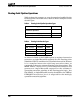
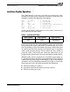
Table 8. Sample 2 – Integer Register and Memory Load Operations
Instruc
Num
Decode
Pipe
Decode
Type
Clocks
Instruction 1 2 3 4 5 6 7 8 9 10 11 12
1DECEDX 0 DP DIE
2 MOV EDI, [ECX] 1 DP D I &/S A $
3 SUB EAX, [EDX+20] 2 DP D I &/S A $/I E
4SAREAX, 5 0 DP D IE
5 ADD ECX, [EDI+4] 1 DP D I &/S A $
6 AND EBX, 0x1F 2 DP D I E
7 MOV ESI, [0x0F100] 0 DP D I & S A $
8 OR ECX, [ESI+EAX*4+8] 1 DP D I &/S A $ E
Comments for Each Instruction Number
1. The ALU operation executes in IEU0.
2. The load operation generates the address in AGU1 and is simultaneously scheduled for the load/store pipe in cycle 3. In
cycles 4 and 5, the load completes the data cache access.
3. The load-execute instruction accesses the data cache in tandem with instruction 2. After the load portion completes, the
subtraction is executed in cycle 6 in IEU2.
4. The shift operation executes in IEU0 (cycle 7) after instruction 3 completes.
5. This operation is stalled on its address calculation waiting for instruction 2 to update EDI. The address is calculated in
cycle 6. In cycle 7/8, the cache access completes.
6. This simple operation executes quickly in IEU2
7. The address for the load is calculated in cycle 5 in AGU0. However, the load is not scheduled to access the data cache
until cycle 6. The load is blocked for scheduling to access the data cache for one cycle by instruction 5. In cycles 7 and 8,
instruction 7 accesses the data cache concurrently with instruction 5.
8. The load execute instruction accesses the data cache in cycles 10/11 and executes the ‘OR’ operation in IEU1 in cycle 12.