
Computer Hardware User Manual


18 AMD Geode™ GX Processor/CS5535 Companion Device GeodeROM Porting Guide
Initialization
32430C
4.1.5.1 GLIU Descriptors Initialization
Register:
P2D_BM, P2D_BMO, P2D_R, P2D_RO, P2D_SC (GLIU0 MSR Address 10000020h-1000003Fh, GLIU1 MSR
Address 40000020h-1000003Fh)
IO_BM, IO_SC (GLIU0 MSR Address 100000E0h-100000FFh, GLIU1 MSR Address 400000E0h-400000FFh)
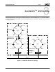
Set up system memory map with GeodeLink Descriptors and Region Control Registers (RConfs). Descriptors and RConfs
must match each other. These register maps will look like the memory map from INT 15h AX = E820.
The responsibility of setting Descriptors and RConfs is split between GeodeROM and VSA technology. GeodeROM han-
dles settings for system memory and VSA memory. Then the responsibility is handed off to VSA technology once it is
loaded to handle all other memory and I/O routing. This is most notable in the frame buffer initialization. See Memory Map,
Figure 7-2 on page 31 for a pictorial representation.
4.1.5.2 GLIU Priority Initialization
Each GeodeLink module has standard MSRs. GLD_MSR_CONFIG is one of the standard registers located at address
2001h in the GX processor and 0001h in the CS5535 companion device. Two fields in some of the GLD_MSR_CONFIG
registers can affect the module priority: Priority Level (PRI0) and Priority Domain (PID). These values default to zero. In the
case of data starvation or saturation on the GLIU, GeodeROM can adjust these values as recommended by AMD.
4.1.5.3 Cache Setup
The GX processor has a 16 KB instruction cache and a 16 KB data cache. The cache is enabled through register CR0 and
both caches can be disabled through MSRs regardless of the CR0 state.
4.1.5.4 Region Configuration
Region Configuration MSRs are used to describe the caching properties of each memory region. Unlike descriptors,
RConfs are designed to overlap. The Default Region Configuration Properties register (CPU Core MSR Address
00001808h) contains the base settings, and RConfs for the shadow area and other special regions supersede its setting.
Example Default Region Configuration Properties:
128 MB memory in the system 8 MB is used for frame buffer and 256 KB is used for VSA technology.
0x1808 = 0x25FFFC02 0x1077DF00
The Default Region Configuration Properties register, shown in Table 4-1, is the main register for GX processor cache set-
tings.
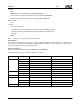
Table 4-1. Default Region Configuration Properties Bit Descriptions
Bit Name (Note) Description
63:56 ROMRP ROM Region Properties. Region properties for addresses greater than ROMBASE (bits
[55:36]).
55:36 ROMBASE ROM Base Address. Base address for boot ROM. This field represents A[32:12] of the
memory address space, for 4 KB granularity.
35:28 DEVRP SYSTOP to ROMBASE Region Properties. Region properties for addresses less than
ROMBASE (bits 55:36]) and addresses greater than or equal to SYSTOP (bits [27:8]).
27:8 SYSTOP Top of System Memory. Top of system memory that is available for general processor
use. The frame buffer and other private memory areas are located above SYSTOP.
7:0 SYSRP System Memory Region Properties. Region properties for addresses less than SYS-
TOP (bits [27:8]). Note that Region Configuration 000A0000h-000FFFFFh takes prece-
dence over SYSRP.
Note: Region Properties: 7:6 = Reserved; 5 = Write Serialize; 4 = Write Combine; 3 = Write-through; 2 = Write Protect;
1 = Write Allocate; 0 = Cache Disable.